Semiconductor Wafer Fab Equipment Market Outlook:
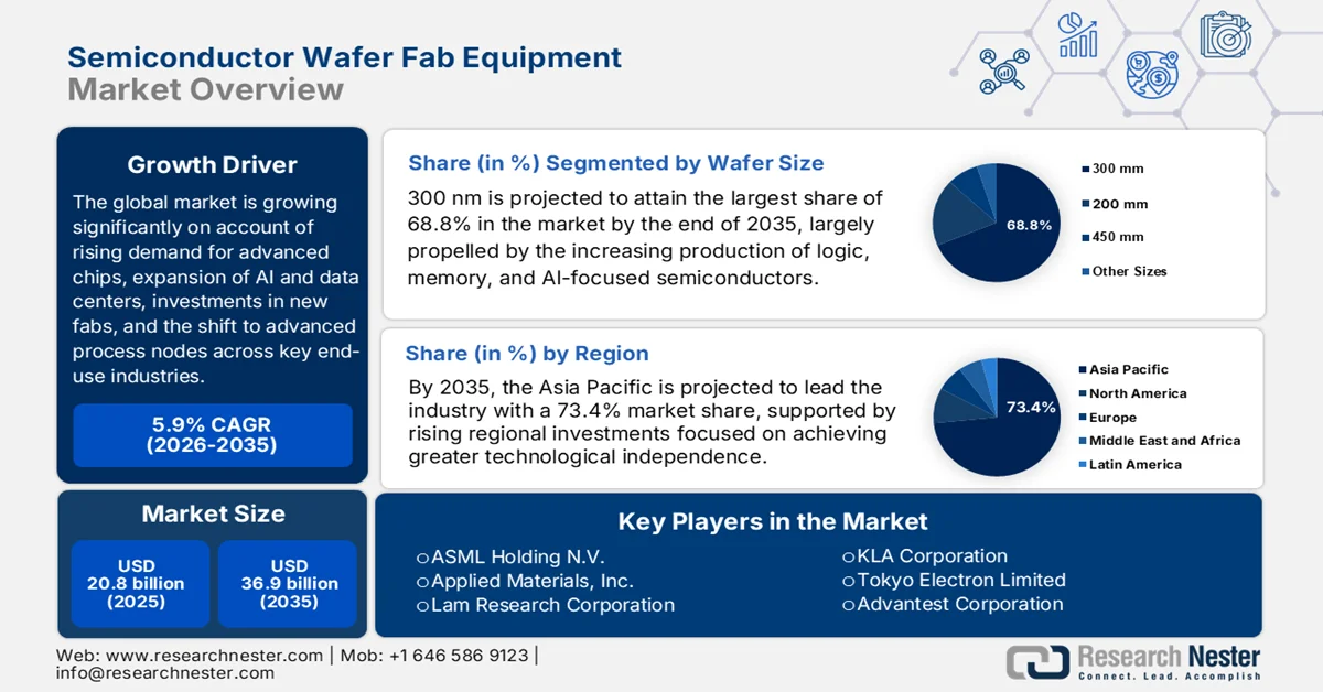
Semiconductor Wafer Fab Equipment Market size was valued at USD 20.8 billion in 2025 and is projected to cross USD 36.9 billion by the end of 2035, growing at more than 5.9% CAGR during the forecast period, i.e., 2026-2035. In 2026, the industry size of semiconductor wafer fab equipment is evaluated at USD 22 billion.
The global semiconductor wafer fab equipment market is projected for notable expansion owing to the unstoppable momentum of artificial intelligence, high-bandwidth memory architectures, and advanced automotive electronics. As foundries globally race to secure technological sovereignty, massive regional manufacturing initiatives are readily accelerating the construction of new fabrication facilities. As per an article published by SEMI Organization in April 2026, global 300mm fab equipment spending is projected to rise 18% to USD 133 billion in 2026 and 14% to USD 151 billion in 2027, marking the first time investments will surpass USD 150 billion. The report also underscored that spending is expected to grow 3% to USD 155 billion in 2028 and 11% to USD 172 billion in 2029, driven by strong AI demand and advanced node expansion, thus denoting a positive market outlook.
Semiconductor Price Indexes Overview: Import, Export, and Producer Manufacturing Trends 2021-2024
Source: BLS
Furthermore, in terms of region, China, Taiwan, Korea, and the Americas will dominate spending, with Japan, Europe & the Middle East, and Southeast Asia also expanding through government incentives and supply chain resilience strategies. Meanwhile, the diversification of semiconductor manufacturing across different nations is prompting increased capacity expansion and the establishment of new fabrication facilities, thereby supporting demand in the semiconductor wafer fab equipment market. Strategic & International Studies in May 2023 stated that the global semiconductor industry has generated a total sale of USD 500 billion in 2022, and semiconductors enable trillions of dollars of economic activity across sectors, from data centers and mobile devices to automobiles and defense systems. The article also stated that the production process involves 500+ stages and supply chains crossing 70+ borders, and the industry is highly complex and globally interdependent. The U.S. leads in terms of design, holding more than 40% of the global IC design market share, whereas the Indo-Pacific, especially Taiwan, Japan, China, and South Korea, has registered itself as a critical hub for manufacturing and supply chain resilience.
Global Semiconductor Equipment Industry Revenue by Region 2024 vs 2023 - Growth Trends and YoY Analysis
|
Region |
2024 Revenue (USD Billions) |
2023 Revenue (USD Billions) |
YoY % Change |
|
China |
49.55 |
36.60 |
+35% |
|
Korea |
20.47 |
19.94 |
+3% |
|
Taiwan |
16.56 |
19.62 |
-16% |
|
North America |
13.69 |
12.05 |
+14% |
|
Japan |
7.83 |
7.93 |
-1% |
|
Europe |
4.85 |
6.46 |
-25% |
|
Rest of the World |
4.19 |
3.65 |
+15% |
|
Total |
117.14 |
106.25 |
+10% |
Source: SEMI
Key Semiconductor Wafer Fab Equipment Market Insights Summary:
Regional Highlights:
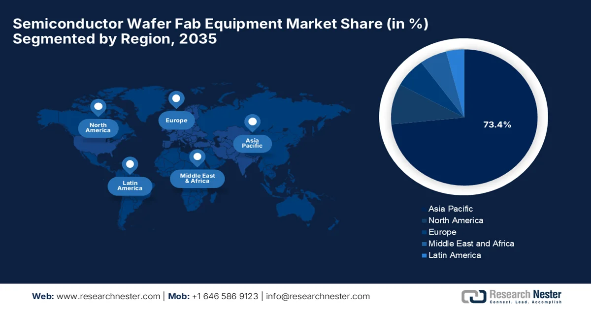
- The asia pacific semiconductor wafer fab equipment market is expected to account for 73.4% of the global share by 2035, underpinned by aggressive investments in semiconductor self-sufficiency and the expansion of next-generation fabrication facilities
- North America is poised to witness robust growth throughout 2026–2035, stimulated by strategic efforts to reshore semiconductor manufacturing and strengthen domestic technology supply chains
Segment Insights:
- In the semiconductor wafer fab equipment market, the 300 mm wafer segment is projected to capture 68.8% share by 2035, reinforced by the accelerating production of logic, memory, and AI-focused semiconductors on cost-efficient high-volume 300 mm wafers
- By 2035, the foundries segment is expected to command a considerable revenue share, supported by the growing outsourcing of chip manufacturing by fabless semiconductor companies and increasing investments in advanced foundry capacity and technology upgrades
Key Growth Trends:
- Proliferation of artificial intelligence and machine learning
- Transition to next-generation chip architectures
Major Challenges:
- Supply chain complexity and geopolitical risks
- Technological complexity and rapid innovation pressure
Key Players: ASML Holding N.V., Applied Materials, Inc., Lam Research Corporation, KLA Corporation, Tokyo Electron Limited, Advantest Corporation, SCREEN Holdings Co., Ltd., Hitachi High-Tech Corporation, Canon Inc., NVIDIA, Taiwan Semiconductor Manufacturing Company (TSMC), Tata Electronics, Nikon Corporation, ASM International N.V., EV Group (EVG), DISCO Corporation, Kokusai Electric Corporation, Onto Innovation Inc., Veeco Instruments Inc., Teradyne Inc., ULVAC, Inc., JEOL Ltd., SÜSS MicroTec SE.
Global Semiconductor Wafer Fab Equipment Market Forecast and Regional Outlook:
Market Size & Growth Projections:
- 2025 Market Size: USD 20.8 billion
- 2026 Market Size: USD 22 billion
- Projected Market Size: USD 36.9 billion by 2035
- Growth Forecasts: 5.9% CAGR (2026-2035)
Key Regional Dynamics:
- Largest Region: Asia Pacific (73.4% Share by 2035)
- Fastest Growing Region: Europe
- Dominating Countries: United States, China, Taiwan, South Korea, Japan
- Emerging Countries: Singapore, India, Germany, Vietnam, Malaysia
Last updated on : 11 June, 2026
Semiconductor Wafer Fab Equipment Market - Growth Drivers and Challenges
Growth Drivers
- Proliferation of artificial intelligence and machine learning: The proliferation of AI and machine learning is efficiently increasing demand for semiconductors. AI accelerators, high-performance processors, and high-bandwidth memory require manufacturing at leading-edge process nodes, which in turn is driving investments in lithography, etching, deposition, and packaging equipment. Apart from this, expanding hyperscale data centers also support sustained wafer fab equipment demand, thus accelerating uptake in the semiconductor wafer fab equipment market. In March 2024, NVIDIA announced the arrival of its Blackwell platform, introducing a breakthrough GPU architecture that is designed to power trillion-parameter AI models with up to 25 times lower cost and energy consumption compared to its predecessor. It consists of innovations such as the GB200 Grace Blackwell Superchip, fifth-generation NVLink, and advanced TensorRT-LLM compiler, and it delivers unmatched performance for generative AI, simulations, and quantum computing. Hence, such instances denote that AI-based semiconductor demand is accelerating investments in advanced wafer fabrication technologies.
- Transition to next-generation chip architectures: Semiconductor manufacturers are opting for technologies such as gate-all-around transistors, chiplet architectures, and 3D integration with a main goal to improve performance and efficiency. These innovations require increasingly sophisticated fabrication processes and higher equipment intensity, driving business in the semiconductor wafer fab equipment market. For instance, in June 2023, Intel announced its breakthrough PowerVia technology, which is the industry’s first implementation of backside power delivery in silicon. It is expected in the Intel 20A node, and the PowerVia moves power wiring to the chip’s backside, solving decades of interconnect bottlenecks and enabling cleaner, more efficient transistor performance. Hence, this innovation marks a radical shift in chipmaking, turning the traditional process two-sided for the first time, thus contributing to wider semiconductor wafer fab equipment market expansion.
Challenges
- Supply chain complexity and geopolitical risks: The global semiconductor wafer fab equipment market is dependent on a very complex and globalized supply chain, which involves precision optics, advanced materials, vacuum systems, and certain specialized components. This makes the market vulnerable to disruptions that are caused by geopolitical tensions, trade restrictions, and export controls. For example, any type of restrictions imposed on advanced semiconductor equipment exports to certain regions have reshaped global semiconductor wafer fab equipment market access and forced companies to redesign supply strategies. Apart from this, dependence on a limited number of specialized suppliers also creates bottlenecks, especially for critical components such as laser systems and EUV optics. In addition, logistics disruptions and regional policy shifts can delay production timelines, due to which companies are pursuing supply chain diversification, localization, and strategic inventory buffering to address these risks.
- Technological complexity and rapid innovation pressure: Another major challenge in the semiconductor wafer fab equipment market is the extreme technological complexity and rapid innovation cycle, which are required to keep pace with Moore’s Law scaling and semiconductor nodes. In this context, equipment manufacturers need to develop tools that are capable of producing smaller, more powerful, and energy-efficient chips, often at atomic-scale precision. Besides, technologies such as high-NA EUV lithography, advanced plasma etching, and sub-nanometer metrology require several years of R&D and massive engineering coordination. Therefore, the risk of technological obsolescence is high, as even slight delays can result in loss of competitive positioning. Moreover, increasing design complexity in chips, which includes 3D architectures and heterogeneous integration, adds to severe pressure on equipment capabilities, negatively impacting the semiconductor wafer fab equipment market’s growth.
Semiconductor Wafer Fab Equipment Market Size and Forecast:
| Report Attribute | Details |
|---|---|
|
Base Year |
2025 |
|
Forecast Year |
2026-2035 |
|
CAGR |
5.9% |
|
Base Year Market Size (2025) |
USD 20.8 billion |
|
Forecast Year Market Size (2035) |
USD 36.9 billion |
|
Regional Scope |
|
Semiconductor Wafer Fab Equipment Market Segmentation:
Wafer Size Segment Analysis
Under the wafer size segment, 300 nm is projected to attain the largest share of 68.8% in the semiconductor wafer fab equipment market by the end of 2035. The segment’s dominance is largely propelled by the increasing production of logic, memory, and AI-focused semiconductors, which are predominantly manufactured on 300 mm wafers due to their superior production efficiency and lower cost per chip. Leading foundries and integrated device manufacturers are expanding 300 mm fabrication capacity to support growing demand. For instance, in June 2024, VIS and NXP announced a joint venture which is called VisionPower Semiconductor Manufacturing Company with the main goal of building a USD 7.8 billion 300mm fab in Singapore. This facility will support 130nm to 40nm mixed-signal, analog, and power management products, with technologies licensed from TSMC, thus denoting a wider segment scope.
Fab Type Segment Analysis
On the basis of fab type, foundries are anticipated to lead with a considerable revenue share in the semiconductor wafer fab equipment market during the forecast period. The segment’s growth is majorly fueled by the rising trend of fabless semiconductor companies outsourcing chip production to specialized foundries, which enables access to advanced process technologies. In addition, significant investments in terms of new foundry facilities and technology upgrades by major manufacturers are increasing demand for lithography, deposition, etching, metrology, and inspection equipment. For instance, in January 2024, Intel and UMC announced a partnership to co-develop a 12nm process platform with FinFET capabilities, which will be manufactured at Intel’s Arizona fabs. This collaboration combines Intel’s U.S. manufacturing scale with UMC’s mature-node expertise, thereby broadening customer access to a geographically diverse and resilient semiconductor supply chain.
Application Segment Analysis
Based on the application, consumer electronics is expected to garner a notable revenue share in the semiconductor wafer fab equipment market during the discussed timeframe. The consistently high demand for smartphones, laptops, wearables, and smart home devices, all of which require advanced semiconductor components, is the main factor behind the subsegment’s leadership. The segment is also driven by rapid product refresh cycles, increasing integration of AI-enabled features in consumer devices, and the shift toward high-performance and energy-efficient chips manufactured on advanced process nodes. For instance, in September 2023, Apple introduced the iPhone 15 Pro and iPhone 15 Pro Max, which consist of aerospace‑grade titanium for a strong yet lightweight design, contoured edges, and a customizable Action button. These devices leverage the A17 Pro chip, which delivers efficient performance, advanced gaming capabilities, and enhanced computational features. The chips are manufactured by utilizing leading-edge semiconductor technology, reflecting a strong dependence on advanced process nodes.
Our in-depth analysis of the semiconductor wafer fab equipment market includes the following segments:
|
Segment |
Subsegments |
|
Wafer Size |
|
|
Fab Type |
|
|
Application |
|
|
Equipment Type |
|
|
Technology Node |
|

Vishnu Nair
Head - Global Business DevelopmentCustomize this report to your requirements — connect with our consultant for personalized insights and options.
Semiconductor Wafer Fab Equipment Market - Regional Analysis
APAC Market Insights
The Asia Pacific semiconductor wafer fab equipment market is anticipated to attain a total share of 73.4% during the forecast period. The region’s leadership is mainly attributable to aggressive domestic investments in technological self-reliance, nations subsidizing and building out next-generation fabrication facilities. The regional surge in demand is also associated with the global leadership of local foundries and memory chipmakers in producing AI hardware, high-bandwidth memory architectures, and complex automotive electronics. For instance, in October 2024, Lam Research inaugurated its Yongin Campus, which is the first global semiconductor equipment company in Korea’s K-semiconductor mega cluster. The site will drive next‑generation R&D and training, supported by Lam’s Semiverse Solutions virtual fabrication platform, thus making it suitable for standard semiconductor wafer fab equipment market growth.
A massive push for technological self-sufficiency and the expansion of domestic manufacturing capacity are certain factors boosting the semiconductor wafer fab equipment market in China. As the country accelerates the buildout of localized supply chains, state-backed investments are driving continuous procurement of mature-node and legacy processing tooling for automotive, industrial, and consumer electronics applications. Based on the government data published in August 2023, China’s Ministry of Industry and Information Technology and Ministry of Finance issued an action plan for stabilizing growth in the electronic information manufacturing industry 2023–2024. This plan targets an average annual growth of 5% in the sector, with revenues surpassing a significant value of USD 3.3 trillion, and sets goals such as 85% 5G mobile phone market share, 25% share for 75-inch+ TVs, and 450 GW of solar cell output. It emphasizes expanding domestic demand, fostering innovation in areas such as VR, advanced computing, and BeiDou applications, and thus heightening the demand for semiconductor wafer fab equipment.
China Semiconductor Manufacturing Equipment Shipments and Imports: 2023-2024 Growth Trends
|
Year |
Metric |
Value |
Change (YoY) |
|
2023 |
China share of global semiconductor equipment spending |
34% |
— |
|
2024 |
China share of global semiconductor equipment spending |
42% |
+8 percentage points |
|
2023 |
China semiconductor manufacturing equipment imports |
USD 42.1 billion (implied) |
— |
|
2024 |
China semiconductor manufacturing equipment imports |
USD 49.2 billion |
+17% YoY |
Source: Silverado
In India, the semiconductor wafer fab equipment market is undergoing significant transformations owing to the presence of suitable government incentives and a national focus on building resilient hardware supply chains. At the same time, the country is attracting significant investments from global tech consortia and domestic conglomerates to establish its first commercial semiconductor fabrication facilities and advanced packaging plants. In February 2024, Tata Electronics announced plans to build India’s first AI-enabled semiconductor fab in Dholera, Gujarat, with technology support from Taiwan’s PSMC. This expansion is backed by a total investment of USD 11 billion. The facility will produce up to 50,000 wafers per month and manufacture chips for automotive, computing, communications, and AI applications. Hence, such instances position the country as a predominant leader in the global semiconductor wafer fab equipment industry.
North America Market Insights
The North America semiconductor wafer fab equipment market has gained enhanced traction over the recent years, majorly driven by a strategic national imperative to reshore critical technology supply chains and secure domestic hardware manufacturing. The regional market is also driven by certain federal and regional subsidies, whereas major global and domestic chipmakers are constructing expansive, next-generation fabrication facilities across the continent. For instance, in March 2024, the Biden-Harris Administration and Intel announced a preliminary agreement for a total of USD 8.5 billion in direct funding under the CHIPS and Science Act. It is combined with a 25% investment tax credit on more than USD 100 billion in planned U.S. investments and eligibility for USD 11 billion in federal loans, and this marks one of the largest public-private commitments in the U.S. semiconductor industry. The initiative will expand Intel’s fabs in Arizona, New Mexico, Ohio, and Oregon, thus strengthening the region’s leadership in AI-era chipmaking.
A concerted federal and state push to revitalize domestic cutting-edge microchip production is driving the semiconductor wafer fab equipment market in the U.S. The presence of massive subsidy frameworks, which are aimed at securing technological leadership and supply chain resilience, and domestic foundry giants are building advanced mega-fab facilities across multiple states, also propels the continued growth of the country’s market. For instance, in April 2024, TSMC Arizona and the U.S. Department of Commerce signed a preliminary agreement for up to USD 6.6 billion in CHIPS Act funding, along with up to USD 5 billion in loans and a 25% investment tax credit. Besides, the company announced plans for a third fab in Phoenix, raising its total U.S. investment to over USD 65 billion, the largest foreign direct investment in Arizona’s history, thus denoting a positive semiconductor wafer fab equipment market outlook.
There is a huge opportunity for Canada semiconductor wafer fab equipment market as it is focused heavily on advanced packaging, photonics, and power electronics manufacturing. The country’s market benefits from targeted national funding and a desire to anchor its position within the regional hardware ecosystem. Canada’s fabrication efforts prioritize specialized wafer processing machinery, advanced chiplet bonding tools, and precision micro-machining equipment, thus rising uptake in this field. In May 2026, Canada announced plans to spin off the Canada Photonics Fabrication Centre into a commercial entity to expand domestic photonic semiconductor manufacturing. It is North America’s only end-to-end pure play compound semiconductor facility, and therefore, CPFC will strengthen Canada’s role in AI innovation and quantum technologies by addressing performance, power, and heat challenges in data centers.
Europe Market Insights
Europe semiconductor wafer fab equipment market is poised for extensive growth in the next decade, propelled by coordinated regional funding initiatives. Both multinational foundry giants and homegrown semiconductor pioneers are building out advanced fabrication facilities and upgrading existing manufacturing sites. This wave of infrastructure spending generates strong demand for specialized wafer processing machinery, particularly high-precision automotive tooling, power electronics fabrication equipment, and next-generation lithography systems. At the same time, the region’s deep-rooted expertise in automotive engineering, industrial automation, and research-grade nanotechnology is efficiently driving a highly specialized equipment market that is focused on producing resilient, mission-critical chips and pioneering advanced architectural scaling.
The Germany semiconductor wafer fab equipment market is experiencing an infrastructure overhaul as the country has registered its position as the premier manufacturing powerhouse of the entire continent. The joint ventures and domestic corporate investments are allowing the country to build out massive cleanroom facilities designed to support high-volume automotive, industrial automation, and green-energy power grids. In this context, the European Commission in June 2025 approved a USD 5.4 billion Germany State aid measure to support the regional Semiconductor Manufacturing Company in building a new chip facility in Dresden. This joint venture between TSMC, Bosch, Infineon, and NXP will produce 480,000 wafers annually using advanced FinFET technology, serving automotive and industrial demand and thus reducing power consumption.
The UK semiconductor wafer fab equipment market is being reshaped by intense focus on compound semiconductors, advanced photonics, and radio-frequency hardware. The presence of targeted national design strategies and a cluster-based manufacturing approach is fostering a favorable business atmosphere for pioneers in this field. This specialized hardware focus generates steady demand for specialized atomic layer etching, plasma-enhanced deposition systems, and precision wafer-bonding machinery, which are suitable for complex, non-silicon architectures. In September 2024, UK Research and Innovation reported that Innovate UK made an investment of USD 14.5 million across 16 projects to boost semiconductor manufacturing and strengthen supply chains in the UK. This funding, part of the national programme, and it supports innovations, new techniques, and collaborations between industry and academia under the UK semiconductor strategy.
Key Semiconductor Wafer Fab Equipment Market Players:
- ASML Holding N.V. (Netherlands)
- Applied Materials, Inc. (U.S.)
- Lam Research Corporation (U.S.)
- KLA Corporation (U.S.)
- Tokyo Electron Limited (Japan)
- Advantest Corporation (Japan)
- SCREEN Holdings Co., Ltd. (Japan)
- Hitachi High-Tech Corporation (Japan)
- Canon Inc. (Japan)
- NVIDIA (U.S.)
- Taiwan Semiconductor Manufacturing Company (TSMC) (Taiwan)
- Tata Electronics (India)
- Nikon Corporation (Japan)
- ASM International N.V. (Netherlands)
- EV Group (EVG) (Austria)
- DISCO Corporation (Japan)
- Kokusai Electric Corporation (Japan)
- Onto Innovation Inc. (U.S.)
- Veeco Instruments Inc. (U.S.)
- Teradyne Inc. (U.S.)
- ULVAC, Inc. (Japan)
- JEOL Ltd. (Japan)
- SÜSS MicroTec SE (Germany)
- Company Overview
- Business Strategy
- Key Product Offerings
- Financial Performance
- Key Performance Indicators
- Risk Analysis
- Recent Development
- Regional Presence
- SWOT Analysis
- ASML Holding N.V. enlists itself as the undisputed leader in the semiconductor wafer fab equipment market and effectively holds a global monopoly in extreme ultraviolet systems, which are essential for advanced node manufacturing below 7nm. The company’s strength is built on decades of deep R&D investment, a highly complex supply chain ecosystem, and tight integration with leading chipmakers.
- Applied Materials, Inc. is the largest diversified semiconductor equipment supplier across the globe, and it has strong positions in deposition, ion implantation, and materials engineering solutions. The company’s strength is structured around multiple stages of the wafer fabrication process, making it a key one-stop supplier for leading fabs.
- Lam Research Corporation is considered to be a dominant player in plasma etch and deposition equipment, which are critical steps in defining intricate circuit patterns on silicon wafers. The company benefits from very strong customer relationships with top foundries and memory manufacturers, particularly in DRAM and NAND flash segments.
- KLA Corporation specializes in terms of process control, metrology, and inspection systems, making it essential for ensuring semiconductor manufacturing precision and yield optimization. The firm is highly focused on defect detection and advanced analytics across the fabrication line.
- Tokyo Electron Limited is one of the most influential Japan-based semiconductor equipment manufacturers, which offers a wide range of products, including coaters/developers, etch systems, and deposition tools. The company competes globally by combining high manufacturing precision with strong cost efficiency and deep collaboration with leading semiconductor fabs.
Here is a list of key players operating in the global semiconductor wafer fab equipment market:
The semiconductor wafer fab equipment market is an extremely consolidated landscape wherein ASML is dominating lithography. On the other hand, Applied Materials, Lam Research, and KLA lead in deposition, etch, and process control systems. Japan-based companies are strong in niche precision tools. Competition in this sector is largely driven by extreme R&D intensity, long development cycles, and deep collaboration with TSMC, Samsung, and Intel. Strategic initiatives opted by the leading pioneers include EUV and High-NA lithography advancement, AI-enabled process optimization, supply chain localization, and capacity expansion. In March 2026, Soitec signed a multi-year agreement to supply POI wafers for Skyworks’ Sky5 platform, for a reliable wafer supply for advanced 5G smartphones. These wafers deliver compactness, robustness, and high performance in dense RF environments, thereby supporting seamless coexistence up to 3+ GHz.
Corporate Landscape of the Semiconductor Wafer Fab Equipment Market:
Recent Developments
- In May 2026, NVIDIA and TSMC are deepening their decades-long partnership by embedding AI directly into semiconductor fabs to accelerate workloads from computational lithography to defect inspection with GPU-powered libraries and vision AI. TSMC leverages platforms such as CUDA-X, Metropolis, and Omniverse, and it is boosting efficiency, yield, and planning agility for next-generation chip manufacturing.
- In May 2026, Tata Electronics and ASML signed a strategic MoU to deploy advanced lithography tools at India’s first 300 mm fab in Dholera for a seamless ramp-up, resilient supply chains, and cutting-edge R&D infrastructure.
- Report ID: 8612
- Published Date: Jun 11, 2026
- Report Format: PDF, PPT
- Explore a preview of key market trends and insights
- Review sample data tables and segment breakdowns
- Experience the quality of our visual data representations
- Evaluate our report structure and research methodology
- Get a glimpse of competitive landscape analysis
- Understand how regional forecasts are presented
- Assess the depth of company profiling and benchmarking
- Preview how actionable insights can support your strategy
Explore real data and analysis
Frequently Asked Questions (FAQ)
Free Sample includes current and historical market size, growth trends, regional charts & tables, company profiles, segment-wise forecasts, and more.
Connect with our Expert


Copyright @ 2026 Research Nester. All Rights Reserved.
