Semiconductor Capital Equipment Market Outlook:
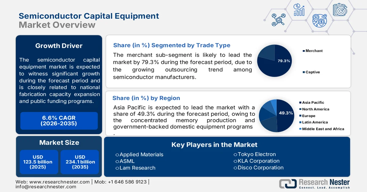
Semiconductor Capital Equipment Market size was valued at USD 123.5 billion in 2025 and is poised to reach USD 234.1 billion by the end of 2035, expanding at around 6.6% CAGR during the forecast period i.e., 2026-2035. In 2026, the industry size of semiconductor capital equipment is evaluated at USD 131.6 billion.
Publicly available government and intergovernmental data indicate that semiconductor capital equipment market demand is closely tied to national fabrication capacity expansion, public funding programs, and technology node transitions. According to the NIST October 2025 data, the U.S. government has committed over USD 52.7 billion in semiconductor manufacturing incentives under the CHIPS and Science Act, including direct funding, loans, and tax credits to support wafer fabrication facilities and equipment procurement. The SIA December 2023 data indicates that the U.S. Department of Commerce reported more than USD 200 billion in announced private semiconductor investments, with a significant portion allocated to front-end fabrication equipment, such as lithography, etch, and deposition tools. These public sector investments are accelerating the fab construction timelines and increasing order visibility for equipment suppliers, particularly in leading-edge and specialty process nodes.
Besides, semiconductor equipment spending is influenced by capacity utilization rates, technology migration cycles, and government-backed resilience strategies. According to the SIA February 2025 data, the global semiconductor sales reached USD 526.8 billion in 2023, reflecting continued demand for advanced chips that necessitate high capital intensity in fabrication processes. Equipment intensity is further supported by the increasing complexity of sub-5 nm and advanced packaging technologies, which require higher tool counts per wafer start. On the other hand, export control measures have imposed restrictions on advanced equipment shipments to certain markets, reshaping global supply chains and redirecting capital expenditure toward compliant regions. Further, these structural factors suggest sustained capital allocation toward semiconductor manufacturing equipment supported by policy-driven localization and technology advancement priorities.
Key Semiconductor Capital Equipment Market Insights Summary:
Regional Highlights:
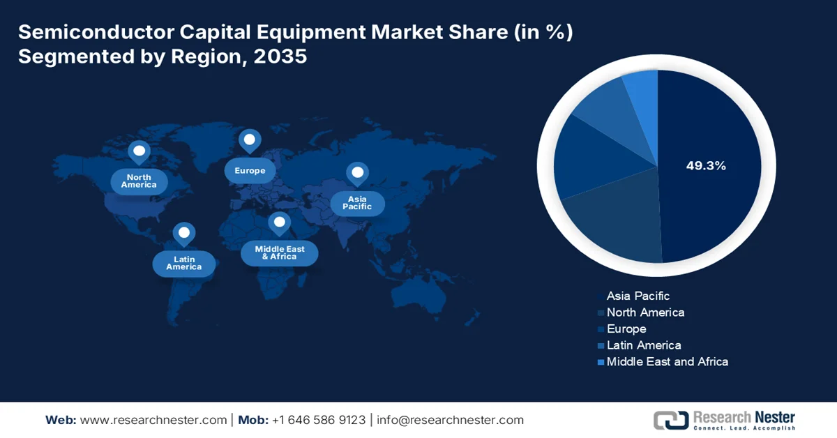
- Asia Pacific is projected to capture 49.3% of the semiconductor capital equipment market share by 2035, driven by expanding foundry investments, concentrated memory production, and government-supported semiconductor self-sufficiency initiatives
- North America is anticipated to register the fastest CAGR of 6.2% during 2026–2035 in the market, stimulated by increasing investments in domestic fabrication capacity and advanced transistor architecture development
Segment Insights:
- The merchant sub-segment is expected to account for 79.3% of the semiconductor capital equipment market by 2035, fueled by rising outsourcing trends among semiconductor manufacturers for fabrication, assembly, and testing operations
- The OEM sub-segment is forecast to maintain its leading position in the market through 2035, supported by growing procurement demand from electric vehicles, 5G infrastructure, and AI-enabled device manufacturers
Key Growth Trends:
- Strategic supply chain localization and resilience policies
- National strategies for advanced packaging
Major Challenges:
- Extreme technological complexity and specialization
- Customer concentration and long qualification cycles
Key Players: Applied Materials (U.S.), ASML (Netherlands), Lam Research (U.S.), Tokyo Electron (Japan), KLA Corporation (U.S.), Disco Corporation (Japan), Teradyne (U.S.), Advantest (Japan), Screen Holdings (Japan), Hitachi High-Tech (Japan), ASM International (Netherlands), Kokusai Electric (Japan), Nikon (Japan), Canon (Japan), Onto Innovation (U.S.), EV Group (Austria), Laser Photonics Corporation (U.S.), ROHM (Japan), Aeluma, Inc. (U.S.), Atomera Incorporated (U.S.).
Global Semiconductor Capital Equipment Market Forecast and Regional Outlook:
Market Size & Growth Projections:
- 2025 Market Size: USD 123.5 billion
- 2026 Market Size: USD 131.6 billion
- Projected Market Size: USD 234.1 billion by 2035
- Growth Forecasts: 6.6% CAGR (2026-2035)
Key Regional Dynamics:
- Largest Region: Asia Pacific (49.3% Share by 2035)
- Fastest Growing Region: North America
- Dominating Countries: United States, China, Japan, South Korea, Taiwan
- Emerging Countries: India, Vietnam, Malaysia, Singapore, Thailand
Last updated on : 14 May, 2026
Semiconductor Capital Equipment Market - Growth Drivers and Challenges
Growth Drivers
- Strategic supply chain localization and resilience policies: Governments are prioritizing supply chain control, leading to geographically diversified semiconductor manufacturing footprints that require duplication of capital equipment. The U.S. highlights the semiconductors as critical to national security, prompting reshoring and friend-shoring strategies. According to the Carnegie Endowment for International Peace, August 2025 data, India approved a USD 10 billion semiconductor incentive program to establish a fabrication and assembly ecosystem. These initiatives are not limited to leading-edge nodes but include mature node capacity critical for automotive and industrial sectors. The result is parallel fab investments across regions, increasing the total equipment demand rather than redistributing it, and also creating opportunities for suppliers to localize service and support infrastructure.
- National strategies for advanced packaging: Governments are increasingly funding the advanced packaging capabilities as part of broader semiconductor strategies, driving demand for back-end capital equipment. According to the U.S. Department of Commerce, January 2025 data, the government has announced USD 1.4 billion in final awards to support the next gen of U.S. Semiconductor advanced packaging. Europe and Japan are also investing in packaging innovation to complement front-end fabrication capabilities. These initiatives are also expanding the scope of the capital equipment demand beyond wafer fabrication to include bonding inspection and testing tools. As heterogeneous integration becomes vital for AI HPC and automotive applications, government-backed packaging ecosystems are emerging as a key growth area for equipment suppliers, with sustained investment expected over the next decade.
U.S. CHIPS Act Investments, 2025
|
Entity / Awardee |
Funding Amount (USD) |
Program / Facility |
|
Absolics, Inc. (Georgia) |
100 million |
SMART Packaging Program |
|
Applied Materials, Inc. (California) |
100 million |
Silicon-core Substrate R&D |
|
Arizona State University (Arizona) |
100 million |
Advanced Electronics & Photonics Core Facility |
|
Natcast (Tempe, Arizona) |
1.1 billion |
NSTC Prototyping & NAPMP Advanced Packaging Piloting Facility (PPF) |
|
CHIPS NAPMP (Program Level) |
300 million |
Materials & Substrates NOFO |
|
U.S. Department of Commerce / CHIPS for America |
Multi-program funding |
National Semiconductor Technology Center (NSTC) |
Source: U.S. Department of Commerce, January 2025
- Rising demand from government supported end use sector: Government spending in strategic sectors such as defense, automotive, electrification, and digital infrastructure is increasing the semiconductor consumption, thereby driving the upstream equipment demand. The U.S. Department of Defense continues to invest heavily in microelectronics for advanced systems, reinforcing domestic semiconductor production needs. Moreover, the public investments in electric vehicles and renewable energy systems across the U.S., EU, and Asia are increasing the demand for power semiconductors and sensors. The growth in EV adoption is supported by the government incentives directly correlate with semiconductor demand. These downstream demand signals translate into higher fab utilization rates and capacity expansion, prompting additional capital equipment purchases to meet long-term supply requirements.
Challenges
- Extreme technological complexity and specialization: Semiconductor equipment represents the pinnacle of precision engineering, requiring mastery across optics, plasma physics, material science, and automation. The industry is moving toward the 3nm and sub-2 nm nodes with gate-all-around transistors demanding atomic layer precision. Moreover, the metrology requirements for 3D structures and advanced packaging have become exponentially more challenging, with measurement gaps in nanostructured materials characterization and backside power delivery networks.
- Customer concentration and long qualification cycles: The semiconductor capital equipment market is extremely concentrated, with TSMC, Samsung, and Intel accounting for a significant percentage of global wafer equipment spending. New players in the face qualification cycles lasting months, requiring on-site testing at customer fabs without guaranteed purchase orders. Even when products technically perform, established equipment vendors have formed solid industrial alliances with major fabs, creating relationship barriers that no amount of technical superiority can easily overcome.
Semiconductor Capital Equipment Market Size and Forecast:
| Report Attribute | Details |
|---|---|
|
Base Year |
2025 |
|
Forecast Year |
2026-2035 |
|
CAGR |
6.6% |
|
Base Year Market Size (2025) |
USD 123.5 billion |
|
Forecast Year Market Size (2035) |
USD 234.1 billion |
|
Regional Scope |
|
Semiconductor Capital Equipment Market Segmentation:
Trade Type Segment Analysis
Under the trade type segment, the merchant sub-segment dominates in the semiconductor capital equipment market and is poised to hold the share value 79.3% by the end of 2035. The segment is driven by the growing outsourcing trend among semiconductor manufacturers that increasingly rely on third-party service providers for fabrication, assembly, and testing. According to the SIA May 2026 data, the global semiconductor sales reached USD 298.5 billion, rising 25% from Q4 2025, while March 2026 sales hit USD 99.5 billion, a 79.2% increase YoY from USD 55.5 billion in March 2025. These data, compiled by the World Semiconductor Trade Statistics, primarily capture merchant semiconductor capital equipment market activity where chips are sold to external customers rather than used internally. With SIA representing 99% of U.S. semiconductor revenue, the data underscores how the merchant players dominate supply, driven by surging demand in AI, automotive, and consumer electronics markets.
Sales Channel Segment Analysis
Within the sales channel segment, the OEM sub-segment leads in the semiconductor capital equipment market. The semiconductor components and equipment are primarily sold directly to the OEMs that integrate them into final products, such as consumer electronics and automotive systems, fostering long-term supplier relationships and stable revenue streams. The U.S. BEA indicates that OEM-driven manufacturing contributed trillions in U.S. durable goods output, highlighting the scale of OEM demand. The rise in electric vehicles, 5G infrastructure, and AI-enabled devices has significantly increased the OEM procurement of front-end equipment. The OEM subsegment remains dominant due to its direct influence on product innovation cycles and large volume purchasing capabilities.
Equipment Type Segment Analysis
The front-end equipment sub-segment remains the most capital-intensive and technologically critical part of the semiconductor value chain and is leading in the equipment type segment. The segment is strongly supported by rising industry investments. According to the SIA 2024 data, U.S. semiconductor firms invested USD 107.5 billion in R&D and capital expenditures in 2023, much of which is directed toward wafer fabrication, lithography, deposition, and etching equipment. These front-end processes are essential for producing advanced nodes required in AI high-performance computing and next-generation communication systems. The increasing demand for the smaller, more efficient chips has driven continuous upgrades in fabrication facilities. This surge in investment highlights the dominance of front-end equipment as manufacturers prioritize innovation, yield improvement, and technological leadership in semiconductor production.
Our in-depth analysis of the semiconductor capital equipment market includes the following segments:
|
Segment |
Subsegments |
|
Equipment Type |
|
|
Technology Node |
|
|
Product Dimension |
|
|
Substrate Material |
|
|
End user Application |
|
|
Trade Type |
|
|
Sales Channel |
|

Vishnu Nair
Head - Global Business DevelopmentCustomize this report to your requirements — connect with our consultant for personalized insights and options.
Semiconductor Capital Equipment Market - Regional Analysis
APAC Market Insights
The Asia Pacific is dominating the semiconductor capital equipment market and is expected to hold the regional revenue share of 49.3% by the end of 2035. The region is driven by concentrated memory production, foundry expansion, and government-backed domestic equipment programs. The key drivers of the semiconductor capital equipment market expansion include China’s pursuit of semiconductor self-sufficiency, Korea’s memory technology leadership, Japan’s materials and deposition equipment strength, and Southeast Asia’s growing back-end assembly footprint. Equipment procurement patterns show front-end tools spending in advanced fabs, and the back-end equipment dominates in Malaysia and the Philippines. Supply chain diversification initiatives are stimulating the equipment purchases in India and Vietnam, where new assembly and test facilities are under construction.
The Japan semiconductor capital equipment market is expanding rapidly, and in 2025, the market reached USD 96.3 million in 2025 and is poised to reach USD 252 million by the end of 2035. Moreover, the market is set to expand at a CAGR of 10.1% during the forecast period. In 2026, the Japan semiconductor capital equipment market is projected to reach USD 106.1 million. The nation is supported by strong government funding, rising domestic production targets, and increasing global demand. According to the ITA November 2025 data, the government has allocated USD 25.7 billion over three years to strengthen the semiconductor sector. KIEP 2026 data shows Japan also aims to achieve USD 99 billion in semiconductor revenue by 2030, supported by USD 79 billion in public and private investment. High external dependency, including 48.3% for integrated circuit inputs, is driving localization efforts, increasing demand for fabrication and materials processing equipment across the semiconductor value chain.
The large-scale investments in fabrication, assembly, and advanced packaging facilities across multiple states are fueling the semiconductor capital equipment market in India. According to the PIB April 2026 data, the cumulative investments exceed USD 19 billion, led by projects such as Tata Electronics’ ₹91,526 crore fab with 50,000 wafer starts per month and Micron’s USD 2.8 billion assembly and test facility supporting DRAM and NAND production. Additional investments in Gujarat, Odisha, and Assam are expanding capabilities in areas such as 3D heterogeneous integration, RF system in package, and silicon carbide manufacturing, all of which require advanced equipment, including lithography, bonding, inspection, and testing systems. Facilities with high production capacities ranging from millions of units per day to thousands of wafers per month indicate strong demand for both front-end and back-end semiconductor capital equipment, positioning India as an emerging manufacturing hub.
North America Market Insights
The North America is projected to emerge as the fastest-growing region in the semiconductor capital equipment market and is expected to expand at a CAGR of 6.2% during the assessed period, 2026 to 2035. The region is driven by its focus on re-establishing domestic leading-edge fabrication capacity and advanced research capabilities. The competitive landscape is shaped by the presence of major original equipment manufacturers, which supply a significant portion of the world’s etch deposition and process control tools. The demand is closely tied to the fabrication facility construction and the transition to new transistor architectures requiring higher equipment intensity per wafer. Mature-node fabs continue to require refurbished tools, while leading-edge facilities drive demand for new high-NA and atomic-layer deposition systems. The overall semiconductor capital equipment market remains sensitive to memory and logic demand cycles.
The federal incentives and complementary private investments targeting advanced semiconductor manufacturing are shaping the semiconductor capital equipment market in the U.S. The U.S. Department of Commerce March 2024 report indicates that USD 8.5 billion in direct funding for Intel to support fab projects across Arizona, New Mexico, Ohio, and Oregon, which are highly equipment-intensive and expected to accelerate the procurement of front-end tools. On the other hand, the April 2024 data shows a proposed USD 6.4 billion CHIPS investment is set to complement over USD 40 billion in private investment for developing a semiconductor cluster in Texas, including leading-edge logic, advanced packaging, and R&D facilities. Additionally, the U.S. BEA February 2025 trade data indicates semiconductors increased by USD 0.7 billion in the recent reporting period, reflecting strengthening domestic production. These developments show a sustained demand for semiconductor capital equipment market across the fabrication and packaging segments.
Canada’s growth in semiconductor capital equipment market is being supported by sustained federal funding, R&D expansion, and concentrated industrial activity. According to Government of Canada data from October 2025, the Strategic Innovation Fund (SIF) has committed USD 8.2 billion in federal contributions, which are linked to USD 72 billion in private-sector investment, creating a strong multiplier effect for semiconductor infrastructure development. These projects support about 113,000 full-time equivalent jobs and reinforce long-term capacity expansion, which drives demand for fabrication, packaging, and testing equipment. Moreover, the SIF-backed initiatives generated USD 1.2 billion in R&D expenditure in 2021, representing about 5% of Canada’s national R&D total, indicating an increasing focus on advanced semiconductor innovation. The Prime Minister of Canada's April 2024 data shows that the federal support of USD 59.9 million for IBM Canada and C2MI further strengthens microelectronics and packaging capabilities. Further, the November 2024 data indicates that Ontario contributing 62.8% of sector GVA, Canada’s semiconductor activity remains geographically concentrated, supporting localized capital equipment deployment and sustained semiconductor capital equipment market growth across advanced manufacturing clusters.
Provincial Distribution of Canada Semiconductor Industry Gross Value Added,2023
|
Province / Region |
Total GVA (USD) |
Share / Contribution Notes |
|
Ontario |
10.2 billion |
62.8% of total GVA; 65.5% of direct impacts; highest concentration ($5.7B direct impact) |
|
Quebec |
2.9 billion |
Significant contributor to national semiconductor output |
|
British Columbia |
1.4 billion |
Moderate contribution to total industry GVA |
|
Alberta |
0.9 billion |
Smaller but notable regional contribution |
|
Combined (QC + BC + AB) |
5.2 billion |
Less than Ontario’s direct impact alone |
Source: Government of Canada November 2023
Europe Market Insights
The combination of regional industrial policy, automotive electronics demand, and specialized research infrastructure is shaping the semiconductor capital equipment market in Europe. Equipment procurement activity concentrates on front-end tools for power semiconductor FD SOI substrates and advanced packaging solutions. The semiconductor capital equipment market benefits from the presence of leading lithography and epitaxy equipment manufacturers headquartered in the region, alongside a network of research consortia that validate new tools for member state fabs. Electric vehicle production requires silicon carbide and gallium nitride processing, as well as defense and aerospace supply chain localization. Back-end equipment for assembly test and packaging also experiences steady uptake due to low barriers to entry compared to front-end segments, which are the active demand drivers. Cross-border equipment qualification programs reduce duplication of certification efforts, enabling faster tool deployment across multiple European fabrication sites.
The large-scale public funding, private investment pipelines, and a robust industrial ecosystem are shaping the semiconductor capital equipment market in Germany. The GTAI 2026 data indicates that the USD 47 billion EU Chips Act and additional USD 22 billion under IPCEI are driving fabrication and technology expansion. Germany alone is expected to attract up to USD 44 billion in public and private semiconductor investments by 2030, directly increasing demand for advanced manufacturing equipment. The industry is projected to generate over USD 19 billion in revenue by 2025, with an anticipated annual growth rate of 10% through 2030, indicating sustained capital expenditure. The Bundeswirtschaftsministerium 2023 data shows Germany also produces more than one-third of Europe’s chips, reinforcing its role as a key manufacturing hub. Furthermore, over USD 23 billion in annual R&D spending in the electrical and digital sector supports continuous innovation, particularly in EUV components and advanced substrates, driving long-term equipment demand.
The steady industry expansion, public investment, and strong productivity within the domestic ecosystem are fueling the semiconductor capital equipment market in the UK. As per the UK Government September 2024 data, the UK semiconductor sector generated USD 12.3 billion in revenue, accounting for 2% of global semiconductor revenues, indicating a stable base for equipment demand, particularly in design-led and specialized manufacturing segments. Moreover, the May 2023 UK Government report shows semiconductor revenue reached USD 601.7 billion in 2022 and is expected to grow at 6% to 8% annually through 2030, reinforcing upstream investment in tools and fabrication technologies. The UK government has also committed USD 384 million in capital investment to the Institute of Technology program, strengthening workforce capabilities essential for advanced semiconductor R&D and production. Additionally, USD 2.2 billion in grants and fundraising secured by semiconductor companies supports innovation and infrastructure, driving continued demand for capital equipment across research, prototyping, and niche production environments.
Key Semiconductor Capital Equipment Market Players:
- Applied Materials (U.S.)
- ASML (Netherlands)
- Lam Research (U.S.)
- Tokyo Electron (Japan)
- KLA Corporation (U.S.)
- Disco Corporation (Japan)
- Teradyne (U.S.)
- Advantest (Japan)
- Screen Holdings (Japan)
- Hitachi High-Tech (Japan)
- ASM International (Netherlands)
- Kokusai Electric (Japan)
- Nikon (Japan)
- Canon (Japan)
- Onto Innovation (U.S.)
- EV Group (Austria)
- Laser Photonics Corporation (U.S.)
- ROHM (Japan)
- Aeluma, Inc (U.S.)
- Atomera Incorporated (U.S.)
- Company Overview
- Business Strategy
- Key Product Offerings
- Financial Performance
- Key Performance Indicators
- Risk Analysis
- Recent Development
- Regional Presence
- SWOT Analysis
- Applied Materials is the largest supplier in the semiconductor capital equipment market, offering a broad portfolio of deposition, etch, and inspection systems. The company uses AI-driven process control and substrate patterning innovations to enable sub-3 nm logic and advanced memory. Strategic initiatives include expanding its EPIC capabilities and securing U.S. CHIPS Act funding to strengthen domestic supply chains.
- ASML holds a near monopoly in extreme ultraviolet lithography, the most critical segment of the semiconductor capital equipment market. Its high NA EUV systems are essential for sub-2 nm nodes, with strategic initiatives focused on raising annual output and deepening co-development with Intel, TSMC, and Samsung. By integrating computational lithography and data analytics, ASML reduces overlay errors. According to the 2024 annual report, the reuse rate of parts is 88%.
- Lam Research specializes in etch deposition and single-wafer clean solutions within the semiconductor capital equipment market. The company’s strategic initiatives emphasize its Sempre technology for 3D NAND and gate-all-around transistors. Lam is aggressively investing in dry resist patterning and cryogenic etch to replace wet processes, reducing environmental impact and cost of ownership.
- Tokyo Electron is Japan’s leading supplier in the semiconductor capital equipment market, excelling in thermal processing, etch, and coat development systems. strategic initiatives include developing ruthenium liner-less CVD for 2nm metallization and pioneering high temperature annealing for power devices. TEL’s AI-powered predictive maintenance and its joint R&D facility with industry partners aim to secure Japan’s re-emergence as a chip equipment powerhouse.
- KLA Corporation dominates the process control and yield management in the semiconductor capital equipment market. strategic initiatives focus on its eSL 10 e beam inspection and reticle inspection systems, which detect nanoscale defects for advanced logic and HNM memory. KLA reduces the false defects and stimulates the root cause analysis. In 2025, the company earned USD 12.2 billion.
Here is a list of key players operating in the global semiconductor capital equipment market:
The semiconductor capital equipment market is highly competitive and is dominated by a few U.S. Japan and Europe giants. Intense R&D investments and vertical integration are key strategic initiatives as players strive to enable sub-3 nm nodes and advanced packaging. The U.S. players use export controls and chip act subsidies, and on the other hand, the Japan leaders focus on materials and deposition synergy. Europe champions highlights lithography and epitaxy niches. Emerging players from South Korea and Malaysia are gaining traction in assembly test and backend equipment. Key strategies include AI-driven process control acquisitions to broaden portfolios and forming co-development pacts with logic memory fabs. For example, in September 2025, Laser Photonics Corporation $LASE, a global leader in industrial laser systems for cleaning and material processing applications, announced that its Beamer Laser Marking Systems subsidiary has received a multi-system order from a top 5 global semiconductor capital equipment company.
Corporate Landscape of the Semiconductor Capital Equipment Market:
Recent Developments
- In April 2026, ROHM has developed a wireless power supply IC chipset consisting of the receiver - ML7670 - and transmitter - ML7671 - compatible with Near Field Communication (NFC) technology for compact wearables such as smart rings and smart bands as well as peripheral devices like smart pens.
- In October 2025, Aeluma, Inc., a semiconductor company specializing in high-performance, scalable technologies for mobile, AI, defense and aerospace, robotics, automotive, AR/VR, and quantum computing, announced that it has acquired significant capital equipment assets from a major components and solutions supplier to expand its prototyping and wafer-scale test capabilities. This investment supports Aeluma’s go-to-market plan and will help qualify manufacturing processes for key target markets.
- In April 2025, Atomera Incorporated, a semiconductor materials and technology licensing company, announced a strategic marketing agreement with a global leader in chip fabrication technology aimed at accelerating the adoption of Atomera’s Mears Silicon Technology™ (MST®) for next-generation technologies, such as AI, 5G and other advanced electronics.
- Report ID: 5322
- Published Date: May 14, 2026
- Report Format: PDF, PPT
- Explore a preview of key market trends and insights
- Review sample data tables and segment breakdowns
- Experience the quality of our visual data representations
- Evaluate our report structure and research methodology
- Get a glimpse of competitive landscape analysis
- Understand how regional forecasts are presented
- Assess the depth of company profiling and benchmarking
- Preview how actionable insights can support your strategy
Explore real data and analysis
Frequently Asked Questions (FAQ)
Free Sample includes current and historical market size, growth trends, regional charts & tables, company profiles, segment-wise forecasts, and more.
Connect with our Expert


Copyright @ 2026 Research Nester. All Rights Reserved.
