Semiconductor Bonding Equipment Market Outlook:
Semiconductor Bonding Equipment Market size was valued at USD 569.2 million in 2025 and is expected to reach USD 935.9 million by the end of 2035, registering around 5.1% CAGR during the forecast period, i.e., 2026-2035. In 2026, the industry size of semiconductor bonding equipment is assessed at USD 598.2 million.
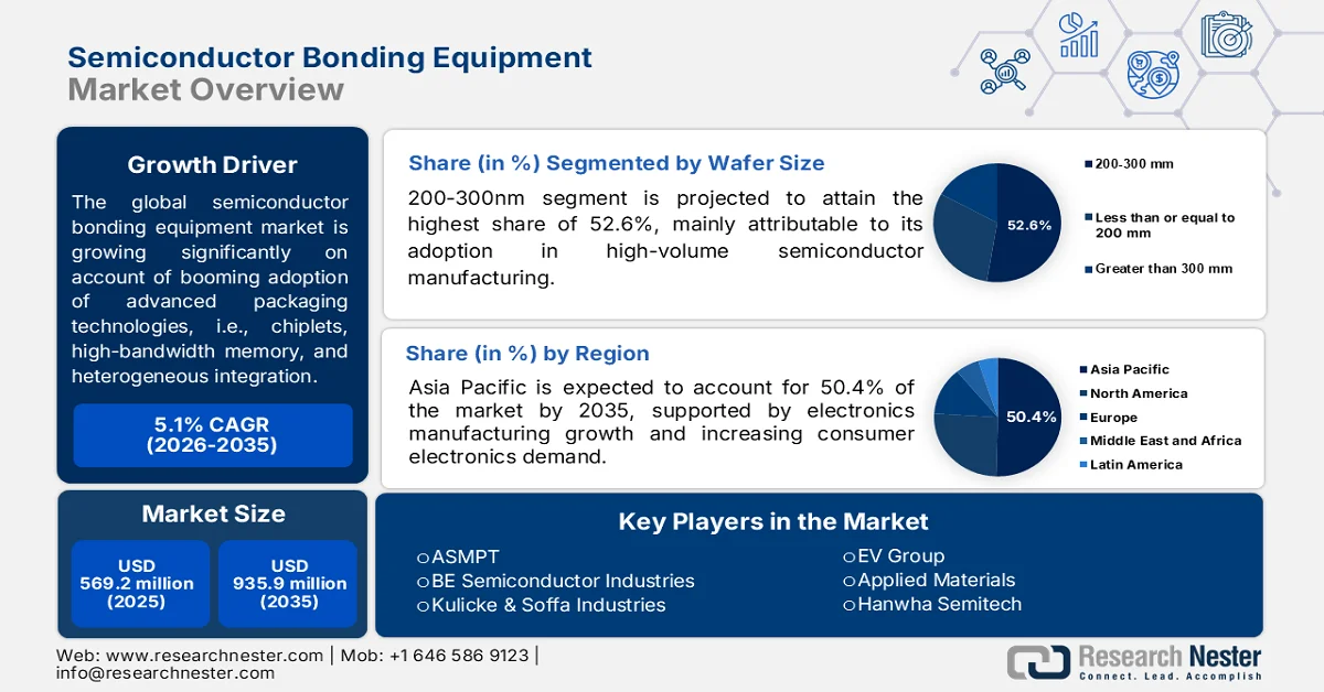
The global semiconductor bonding equipment market is growing at a significant rate based on factors including the booming adoption of advanced packaging technologies, i.e., chiplets, high-bandwidth memory, and heterogeneous integration. This surge is fueled by the rising demand for high-performance computing, automotive electronics, as well as mobile devices. In January 2025, the U.S. Department of Commerce allocated a generous amount of USD 1.4 billion through the CHIPS national advanced packaging manufacturing program to strengthen domestic semiconductor packaging capabilities. This funding includes support for Applied Materials, Absolics, Arizona State University, and Natcast to advance substrate technologies, 3D integration, fan-out packaging, and large-scale packaging research, thus building a stronger U.S. advanced packaging ecosystem.
Furthermore, the semiconductor bonding equipment market depends on the availability of raw materials such as silicon wafers, copper, dielectric materials such as SiO₂ or SiCN, metals, ceramics, specialty chemicals, gases, and semiconductor-grade adhesives. In February 2026, the SEMI Organization disclosed that worldwide silicon wafer shipments rose 5.8% in 2025 to 12,973 million square inches, whereas wafer revenue declined 1.2% to USD 11.4 billion, marking a recovery in shipment volumes after the previous downturn. This growth was driven mainly by strong AI-related demand for advanced epitaxial wafers used in logic and polished wafers supporting high-bandwidth memory, whereas traditional semiconductor applications continued to face weak demand and pricing pressure, underscoring an urgent need for reliable and cost-effective access to high-quality semiconductor-grade raw materials.
Key Semiconductor Bonding Equipment Market Insights Summary:
Regional Highlights:
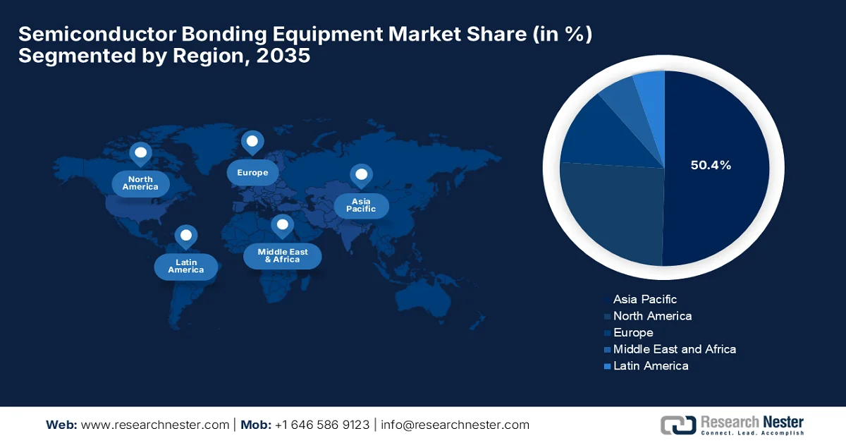
- Asia Pacific is projected to command a 50.4% share of the semiconductor bonding equipment market by 2035, supported by expanding electronics manufacturing, rising demand for advanced packaging technologies, and the proliferation of consumer electronics, automotive electronics, and high-performance computing devices
- North America is positioned for significant growth through 2035, fueled by strong research and development activity and rising demand for complex chip architectures such as chiplets and 3D stacked dies
Segment Insights:
- The 200-300nm segment is projected to account for a leading 52.6% share of the semiconductor bonding equipment market by 2035, owing to its widespread adoption in high-volume semiconductor manufacturing and its balance of production efficiency, manufacturing costs, and chip yield
- The thermocompression segment is anticipated to secure a considerable share by 2035, propelled by increasing adoption in advanced semiconductor packaging, particularly die-to-wafer applications requiring precise and reliable interconnections
Key Growth Trends:
- Surging proliferation of generative AI
- Increasing investments in semiconductor manufacturing capacity
Major Challenges:
- Long qualification cycles and yield requirements
- Supply chain and component constraints
Key Players: ASMPT (Singapore) ,BE Semiconductor Industries (Besi) (Netherlands) ,Kulicke & Soffa Industries (Singapore) ,EV Group (Austria) ,Applied Materials (U.S.) ,Hanwha Semitech (South Korea) ,Shibaura Mechatronics (Japan) ,SUSS MicroTec (Germany) ,SET Corporation (France),Imec (Belgium).
Global Semiconductor Bonding Equipment Market Forecast and Regional Outlook:
Market Size & Growth Projections:
- 2025 Market Size: USD 569.2 million
- 2026 Market Size: USD 598.2 million
- Projected Market Size: USD 935.9 million by 2035
- Growth Forecasts: 5.1% CAGR (2026-2035)
Key Regional Dynamics:
- Largest Region: Asia Pacific (50.4% Share by 2035)
- Fastest Growing Region: North America
- Dominating Countries: China, Taiwan, South Korea, Japan, United States
- Emerging Countries: India, Germany, Netherlands, Singapore, Malaysia
Last updated on : 20 August, 2026
Semiconductor Bonding Equipment Market - Growth Drivers and Challenges
Growth Drivers
- Surging proliferation of generative AI: The explosive growth of generative AI infrastructure and high-performance computing needs chips that possess massive data bandwidth and processing power. This demand directly accelerates the deployment of high-precision bonding equipment. It is essential for fabricating the dense interconnected architectures that are found in modern GPU accelerators and neural processing units. In December 2023, India Brand Equity Foundation revealed that generative AI is emerging as a major driver of productivity, automation, and innovation, and India’s Gen AI industry is projected to reach USD 51.8 billion by 2028. It also outlines that for technology services, Gen AI could expand the addressable market by 15% to 20%, and generate gains in corporate functions through automation and AI-powered solutions, thus driving growth in the market.
- Increasing investments in semiconductor manufacturing capacity: Governments and semiconductor companies across the globe are making substantial investments in domestic chip manufacturing facilities to strengthen supply chains. New fabrication plants and advanced packaging facilities require modern assembly and bonding equipment, thus creating sustained opportunities for bonding equipment suppliers as well as technology developers. In January 2024, Intel inaugurated a Fab 9 in Rio Rancho, New Mexico, as part of its USD 3.5 billion investment to expand high-volume manufacturing of advanced semiconductor packaging technologies. This facility enables mass production of Intel’s Foveros 3D packaging technology, which vertically stacks chiplets to improve performance, power efficiency, and cost, thus making it suitable for driving the market.
Challenges
- Long qualification cycles and yield requirements: Lengthy qualification cycles and stringent yield requirements are considered to be a major challenge for manufacturers in the market. Semiconductor customers require extensive testing before introducing new bonding equipment into high-volume manufacturing, as equipment performance can directly influence device reliability and overall production yield. Meanwhile, advanced bonding processes might require lengthy optimization of bonding force, temperature, alignment, surface preparation, pressure, and process timing. Any equipment change can therefore require substantial process requalification. This in turn creates barriers for new suppliers who are attempting to enter the market and strengthens relationships between established equipment manufacturers and major semiconductor producers.
- Supply chain and component constraints: Semiconductor bonding equipment manufacturers depend on certain precision components, motion-control systems, optical alignment technologies, sensors, vacuum systems, robotics, and specialized electronics. Besides, any type of disruption affecting these components can delay equipment production and customer installations, and the challenge becomes more intense as bonding systems require precise and specialized components that might not have well-qualified suppliers. On the other hand, geopolitical tensions, export controls, transportation disruptions, and fluctuations in semiconductor capital-equipment demand can also negatively affect procurement and manufacturing schedules. Therefore, companies in the market need to maintain reliable supplier networks while controlling inventory and production costs.
Semiconductor Bonding Equipment Market Size and Forecast:
| Report Attribute | Details |
|---|---|
|
Base Year |
2025 |
|
Forecast Year |
2026-2035 |
|
CAGR |
5.1% |
|
Base Year Market Size (2025) |
USD 569.2 million |
|
Forecast Year Market Size (2035) |
USD 935.9 million |
|
Regional Scope |
|
Semiconductor Bonding Equipment Market Segmentation:
Wafer Size Segment Analysis
On the basis of wafer size, 200-300nm segment is projected to attain the highest share of 52.6% in the semiconductor bonding equipment market from 2026 to 2035. The sub-segment’s leadership in this sector is mainly attributable to its adoption in high-volume semiconductor manufacturing, as they offer an optimal balance between production efficiency, manufacturing costs, and chip yield. Their compatibility with established fabrication infrastructure and advanced bonding processes further supports their continued dominance. For instance, EV Group in March 2025 introduced the GEMINI® automated wafer bonding system, which is designed for 300-mm MEMS manufacturing, and it consists of a newly engineered high-force bond chamber to improve bonding quality and production yield across larger wafer surfaces. This system supports bond forces of up to 350 kN, high-vacuum processing, overpressure capability, automated optical alignment, and flexible configurations for various wafer-bonding techniques.
Bonding Technology Segment Analysis
By the conclusion of the forecast period, the thermocompression segment is anticipated to attain a considerable share in the market. The sub-segment’s growth is mainly propelled by the increasing adoption of thermocompression bonding for advanced semiconductor packaging which is particularly die-to-wafer applications, where it enables precise and reliable interconnections for high-performance devices. BE Semiconductor Industries N.V. in March 2025 announced a follow-on order which was worth USD 20 million for five TCB Next thermo-compression bonding systems from a major semiconductor manufacturer. The order reflects growing industry adoption of Besi’s TCB Next die-to-wafer bonding technology, which is designed for advanced wafer-level semiconductor assembly applications.
Equipment Type Segment Analysis
Permanent bonding equipment is expected to grow with a substantial revenue share in the market during the stipulated timeframe. Increasing adoption of wafer bonding in high-volume semiconductor and MEMS manufacturing, the growing demand for 3D and heterogeneous integration, and the need for reliable, high-yield bonding across larger wafer surfaces are positioning the sub-segment for sustained growth. In addition, the continued development of automated production bonding platforms is also supporting market expansion, as manufacturers look for greater throughput, process consistency, and cost efficiency. In June 2024, EV Group and Fraunhofer IZM-ASSID expanded their collaboration to develop advanced wafer bonding and debonding technologies for heterogeneous integration, including applications in quantum computing. This partnership begins with the installation of EVG’s EVG850 DB automated UV laser debonding and cleaning system at CEASAX in Dresden, supporting 300-mm wafer-scale research and enabling in-house processing of thin and fragile semiconductor structures.
Our in-depth analysis of the semiconductor bonding equipment includes the following segments:
|
Segment |
Subsegments |
|
Wafer Size |
|
|
Bonding Technology |
|
|
Equipment Type |
|
|
Application |
|
|
End user |
|

Vishnu Nair
Head - Global Business DevelopmentCustomize this report to your requirements — connect with our consultant for personalized insights and options.
Semiconductor Bonding Equipment Market - Regional Analysis
APAC Market Insights
Asia Pacific semiconductor bonding equipment market is forecasted to attain the highest share of 50.4% during the assessed timeframe. The region’s upliftment in this sector is mainly propelled by expansion of the electronics manufacturing sector, increasing demand for advanced packaging technologies, and the proliferation of consumer electronics, automotive electronics, and high-performance computing devices. Asia Pacific is considered to be a major hub for semiconductor manufacturing and assembly, in which the key countries are continuously investing in manufacturing infrastructure and packaging facilities. In August 2025, the Press Information Bureau stated that India is building its semiconductor ecosystem through the India Semiconductor Mission, with almost USD 17 billion in approved projects across six states, covering chip fabrication, packaging, design, and advanced technologies.
The government's intense focus on domestic semiconductor self-sufficiency and extensive investments in local manufacturing infrastructure are the main factors driving the growth of the market in China. This growth is also being supported by the country's consumer electronics fabrication base, along with the booming electric vehicle sector, and the widespread deployment of advanced telecommunications infrastructure. In this context, Shanghai University published an international tender in September 2024 for the procurement of one wafer bonding machine and the equipment to be installed in Shanghai, and funding was already secured. This tender required suppliers to be original manufacturers or authorized agents with established sales and maintenance support in mainland China and thus positively contributing to the market’s expansion.
The Japan semiconductor bonding equipment market is growing exponentially owing to the nation’s legacy of precision engineering and its strategic position as a primary global supplier of advanced semiconductor materials and components. In addition, the country’s focus on research and development, backed by government initiatives to revitalize domestic chip fabrication infrastructure, is supporting a steady demand for ultra-precise and automated bonding machinery. Based on government data published in March 2024, Japan is investing heavily in Rapidus to establish domestic production of advanced 2-nm semiconductors, with a significant USD 2.2 billion in government support and about USD 49 million from major domestic companies. In this context, Rapidus is partnering with IBM and imec to launch a pilot line and begin mass production, thus suitable for bolstering the market’s growth.
North America Market Insights
The North America market is predicted to grow with a considerable share during the discussed time period. The region benefits from a strong emphasis on research, development, and high-performance computing applications. The market is effectively driven by an ecosystem of fabless design companies, defense aerospace contractors, and tier-one cloud service providers that require complex chip architectures such as chiplets and 3D stacked dies. In September 2025, the National Institute of Standards and Technology developed an advanced wafer-bonding method for heterogeneous integration that enables different semiconductor materials and components to be combined into compact, high-performance devices. In addition, it also stated that this particular technique uses precisely formed pockets and protective stop layers in order to accommodate uneven surfaces and enable reliable bonding of multiple wafer layers without damaging any existing structures.
A national focus to rebuild a secure domestic supply chain and lead in next-generation microelectronics architecture is driving growth of the U.S. semiconductor bonding equipment market. The country’s market also benefits from the soaring requirements of AI, high-performance computing, and aerospace systems, which depend on packaging techniques such as 3D die stacking and chiplets. In April 2025, Intel Foundry outlined progress in advanced process technology, packaging, and manufacturing. It also mentioned the key developments, which include Intel 14A, 18A, and advanced variants, along with Foveros Direct hybrid bonding, EMIB-T, and new 3D/2.5D packaging technologies for high-performance chip integration.
The Canada semiconductor bonding equipment market has a huge opportunity to grow in the upcoming years owing to the nation’s strategic focus on specialized niche sectors such as photonics, micro-electromechanical systems, and advanced sensor technologies. The market is driven by a strong network of university-linked research hubs, incubator ecosystems, and fabrication facilities that support the automotive, aerospace, and biomedical industries. Based on the government data published in January 2026, Canada is strengthening its semiconductor industry by focusing on specialized areas such as compound semiconductors, advanced packaging, photonics, and semiconductor R&D. The supportive government initiatives include USD 43.1 million for IBM Canada and C2MI, USD 25.9 million for Ranovus, and USD 180 million for semiconductor projects.
Europe Market Insights
The Europe market is growing significantly, which is propelled by a strong focus on automotive electronics, industrial automation, and power management sectors. The regional market also benefits from a well-established automotive supply chain and the rapid transition toward electric vehicles, which demand highly reliable power semiconductors such as silicon carbide and gallium nitride. In May 2024, STMicroelectronics announced a generous investment of USD 5.4 billion to build a fully integrated 200-mm silicon carbide (SiC) manufacturing campus in Catania, Italy, for substrate production, wafer fabrication, testing, and packaging. This project includes around USD 2.2 billion in support from the government of Italy under the EU Chips Act.
The country’s industrial automation and power electronics manufacturing are fueling growth in the Germany semiconductor bonding equipment market. The rapid shift toward renewable energy systems fuels a strong demand for highly reliable power semiconductors, such as silicon carbide and gallium nitride, which require specialized, heat-resistant bonding technologies. In this context, the European Commission in July 2026 approved USD 770 million in the country’s state aid for four new semiconductor facilities by covering SiC epi-wafers, power MOSFETs, advanced metrology equipment, and specialized chips. This funding includes USD 407.3 million for Element 3-5, USD 246.9 million for Vishay, USD 85.9 million for KLA, and USD 20.7 million for KETEK, thus strengthening the region’s semiconductor manufacturing capacity and supply-chain resilience.
The UK semiconductor bonding equipment market is projected to witness surging growth, which is driven by a well-established tech ecosystem, especially structured around research clusters that support advanced applications. Government-backed microelectronics initiatives and strategic funding are readily boosting local open-access foundry capabilities and advanced packaging prototyping. In May 2026, the University of Strathclyde awarded an USD 1.1 million contract to Inseto UK Limited for the supply, delivery, and installation of a sinter bonding system for semiconductor advanced packaging research. This equipment will support the National Manufacturing Institute Scotland (NMIS) in developing and scaling power semiconductor packaging, including die-to-substrate, substrate-to-heatsink, and double-sided cooling applications, thus positively benefiting the market’s expansion.
Key Semiconductor Bonding Equipment Market Players:
- ASMPT (Singapore)
- BE Semiconductor Industries (Besi) (Netherlands)
- Kulicke & Soffa Industries (Singapore)
- EV Group (Austria)
- Applied Materials (U.S.)
- Hanwha Semitech (South Korea)
- Shibaura Mechatronics (Japan)
- SUSS MicroTec (Germany)
- SET Corporation (France)
- Imec (Belgium)
- Company Overview
- Business Strategy
- Key Product Offerings
- Financial Performance
- Key Performance Indicators
- Risk Analysis
- Recent Development
- Regional Presence
- SWOT Analysis
- ASMPT is a leading bonding-equipment manufacturer which is offering AMICRA die and flip-chip bonders for advanced packaging, 3D stacking, TSV, WLP, MEMS, and silicon photonics. The company’s systems emphasize high placement accuracy, automation, and production flexibility.
- BE Semiconductor Industries holds a strong position in advanced hybrid bonding effectively propelled through its Datacon platforms. The firm’s equipment focuses on high-accuracy, high-throughput bonding for high-density interconnects, 3D integration, and advanced packaging.
- Kulicke & Soffa Industries is a prominent player in this sector, and it provides thermo-compression bonding equipment for ultra-fine-pitch semiconductor packaging. Its technologies efficiently support high-density interconnects, heterogeneous integration, copper-to-copper bonding, AI, along with high-performance computing applications.
- EV Group specializes in wafer bonding equipment, which includes its GEMINI automated production platform. Besides, its solutions support wafer-to-wafer alignment and bonding for advanced packaging, 3D integration, MEMS, and high-volume manufacturing.
- Applied Materials competes in advanced hybrid bonding through its Kinex integrated die-to-wafer system, which is developed in collaboration with Besi. This platform targets HBM, 3D ICs, chiplets, photonics, and advanced logic, combining bonding precision, cleaning, activation, and metrology capabilities.
Here is a list of key players operating in the global market:
The semiconductor bonding equipment market is being led by global suppliers with broad die-bonding, flip-chip, thermo-compression, wafer-bonding, and hybrid-bonding portfolios. ASMPT, Besi, Kulicke & Soffa, EV Group and Applied Materials compete intensely in this industry through precision placement, throughput, process integration and advanced hybrid-bonding capabilities. On the other hand, regional specialists including Shibaura Mechatronics, Hanwha Semitech, SUSS MicroTec and SET strengthen competition in advanced packaging, wafer-level and high-precision applications. In April 2025, Applied Materials acquired a 9% stake in BE Semiconductor Industries (Besi) with the main goal of strengthening their long-term partnership in hybrid bonding technology. The companies are developing an integrated die-based bonding system that is especially designed to support high-volume manufacturing of advanced semiconductor packaging.
Corporate Landscape of the Market:
Recent Developments
- In May 2026, Imec and EV Group demonstrated wafer-to-wafer hybrid bonding at a 200 nm interconnect pitch, and it achieved a highly accurate alignment across a full 300 mm wafer. The supports advanced 3D chip designs, including logic-to-logic and memory-to-logic stacking.
- In October 2025, Applied Materials introduced new semiconductor manufacturing technologies that are designed to improve the performance and energy efficiency of AI-focused chips. The company’s Kinex™ hybrid bonding system supports advanced chip stacking, whereas Xtera™ and PROVision™ technologies improve transistor fabrication and 3D chip inspection.
- Report ID: 8739
- Published Date: Aug 20, 2026
- Report Format: PDF, PPT
- Explore a preview of key market trends and insights
- Review sample data tables and segment breakdowns
- Experience the quality of our visual data representations
- Evaluate our report structure and research methodology
- Get a glimpse of competitive landscape analysis
- Understand how regional forecasts are presented
- Assess the depth of company profiling and benchmarking
- Preview how actionable insights can support your strategy
Explore real data and analysis
Frequently Asked Questions (FAQ)
About this Report
Connect with our Expert


Report, 2026-2035


Copyright @ 2026 Research Nester. All Rights Reserved.
