Extreme Ultraviolet (EUV) Lithography Market Outlook:
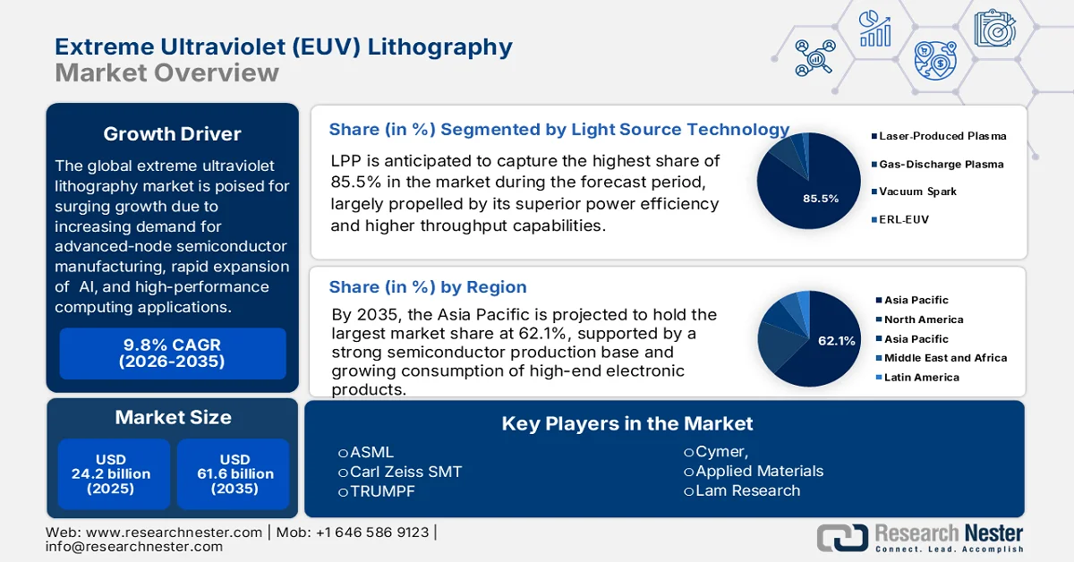
Extreme Ultraviolet (EUV) Lithography Market size was valued at USD 24.2 billion in 2025 and is anticipated to reach USD 61.6 billion by the end of 2035, expanding at around 9.8% CAGR during the forecast period, i.e., between 2026-2035. In 2026, the industry size of extreme ultraviolet lithography is estimated at USD 26.5 billion.
The global extreme ultraviolet lithography market is experiencing exceptional growth owing to the insatiable global demand for advanced semiconductors to power artificial intelligence accelerators, high-performance computing, and next-generation mobile devices. Foundries and integrated device manufacturers across the globe are continuously expanding their advanced-node manufacturing facilities, thereby establishing EUV technology as the mandatory foundation for sub-3nm and sub-2nm mass production. As per an article published by Semiconductor Industry Association (SIA) in June 2026, global semiconductor sales surged to a substantial USD 110.5 billion in April 2026, which marks an 11% increase from March and a massive 93.9% jump year-over-year. The SIA also projects that annual sales will reach USD 1.5 trillion by the end of 2026, effectively fueled by demand for AI infrastructure and accelerated computing platforms. Regionally, growth was strongest in the Americas and Asia Pacific, wherein all major markets showed robust momentum, thus highlighting the industry’s rapid expansion toward a projected USD 1.9 trillion in 2027.
Furthermore, growth in the extreme ultraviolet (EUV) lithography market is being accelerated by the commercial deployment of high-numerical-aperture EUV systems, which enable transistor scaling and eliminate the need for complex multi-patterning processes. In addition, the presence of strong government subsidies and national security initiatives worldwide is pushing for localized semiconductor supply chains, guaranteeing sustained investment in EUV hardware, advanced reflective photomasks, and specialized chemical photoresists for years to come. In April 2024, Intel reported that it installed and began calibration of the world’s first High NA EUV lithography tool at its Fab D1X in Oregon. It is built by ASML, and the 165-ton TWINSCAN EXE:5000 system delivers unprecedented resolution and feature scaling, enabling Intel Foundry to extend Moore’s Law beyond Intel 18A. Hence, such technology is expected to drive advancements in AI and emerging applications, positively impacting the market’s expansion.
Key Extreme Ultraviolet (EUV) Lithography Market Insights Summary:
Regional Highlights:
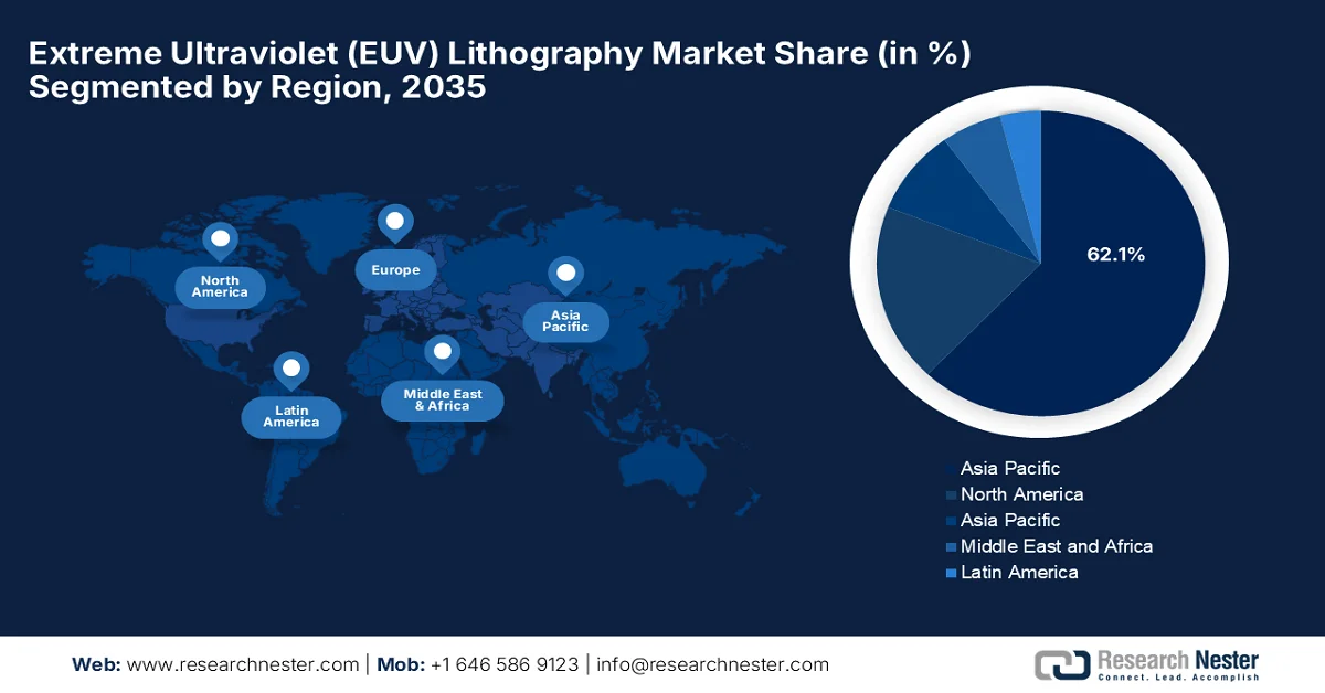
- The extreme ultraviolet (euv) lithography market in Asia Pacific is projected to secure 62.1% share by 2035, reinforced by the semiconductor manufacturing ecosystem and rising consumer demand for advanced electronic devices
- North America is anticipated to strengthen its position across the forecast period, supported by strong federal backing for domestic high-tech supply chains
Segment Insights:
- The laser-produced plasma segment in the extreme ultraviolet (euv) lithography market is expected to account for 85.5% share by 2035, fueled by superior power efficiency, higher throughput capabilities, and expanding adoption across advanced semiconductor manufacturing processes
- Light sources under the product type segment are projected to maintain a considerable market share by 2035, supported by continuous advancements in high-power EUV light-source technologies, increasing investments in next-generation High-NA EUV systems, and rising demand for higher wafer throughput and improved patterning precision in advanced semiconductor manufacturing
Key Growth Trends:
- AI and accelerator proliferation
- Expansion of smartphones and consumer electronics
Major Challenges:
- Technical complexity and yield optimization
- Limited supplier base and supply chain concentration
Key Players: ASML (Netherlands) ,Carl Zeiss SMT (Germany) ,TRUMPF (Germany) ,Cymer (U.S.) ,Applied Materials (U.S.) ,Lam Research (U.S.) ,KLA Corporation (U.S.) ,Tokyo Electron Limited (Japan) ,Hitachi High-Tech Corporation (Japan) ,Nikon Corporation (Japan) ,Canon Inc. (Japan) ,Taiwan Semiconductor Manufacturing Company (Taiwan) ,Samsung Electronics (South Korea) ,Intel Corporation (U.S.) ,SK Hynix Inc. (South Korea) ,JSR Corporation (Japan) ,Shin-Etsu Chemical Co., Ltd. (Japan) ,Fujifilm Holdings Corporation (Japan) ,Qnity Electronics (U.S.) ,SCREEN Semiconductor Solutions (Japan) ,IBM (U.S.) ,DuPont de Nemours, Inc. (U.S.) ,Merck Group / EMD Electronics (Germany).
Global Extreme Ultraviolet (EUV) Lithography Market Forecast and Regional Outlook:
Market Size & Growth Projections:
- 2025 Market Size: USD 24.2 billion
- 2026 Market Size: USD 26.5 billion
- Projected Market Size: USD 61.6 billion by 2035
- Growth Forecasts: 9.8% CAGR (2026-2035)
Key Regional Dynamics:
- Largest Region: Asia Pacific (62.1% Share by 2035)
- Fastest Growing Region: North America
- Dominating Countries: United States, Taiwan, South Korea, Japan, China
- Emerging Countries: Netherlands, Germany, India, Singapore, France
Last updated on : 11 June, 2026
Extreme Ultraviolet (EUV) Lithography Market - Growth Drivers and Challenges
Growth Drivers
- AI and accelerator proliferation: Hyperscale data centers are the main factors responsibly fueling demand for AI accelerators, i.e., GPUs and TPUs. These chips require extreme transistor density to handle large-scale model training and inference. In this context, EUV lithography enables fabrication at advanced nodes, allowing billions of transistors on a single die while maintaining power efficiency and performance. For instance, in August 2023, NVIDIA unveiled its GH200 Grace Hopper Superchip platform, which is especially designed for accelerated computing and generative AI workloads in hyperscale data centers, including large language models and recommender systems. This particular platform delivers up to 8 petaflops of AI performance and 282GB of HBM3e memory, enabling significantly higher memory bandwidth and model capacity. Hence, this reflects growing AI-based demand for advanced chip designs manufactured using EUV-enabled leading-edge semiconductor nodes, benefiting the overall extreme ultraviolet lithography market.
- Expansion of smartphones and consumer electronics: The worldwide demand for smartphones, tablets, wearables, and smart home devices has been rising continuously, which encourages semiconductor manufacturers to adopt EUV lithography. Companies depend on advanced chips to deliver higher performance and enhanced AI capabilities in compact consumer devices, thus driving the expansion of the extreme ultraviolet (EUV) lithography market. As per an article published by the World Economic Forum in April 2023, mobile phones have become more numerous than people, with over 8.58 billion subscriptions worldwide in 2022, when compared to a global population of 7.95 billion. This milestone reflects the explosive growth, and in 2023, 5.4 billion people have at least one mobile subscription, highlighting the ubiquity of mobile technology. The trend supports continued demand for extreme ultraviolet lithography solutions.
Challenges
- Technical complexity and yield optimization: EUV lithography consists of some advanced and sensitive technology, which makes process control and yield optimization extremely challenging. The system operates at a 13.5 nm wavelength, which requires near-perfect vacuum conditions and ultra-precise optical components. Even any type of minor contamination or vibration can negatively impact wafer quality and reduce yield rates. In addition, any type of resist materials used in EUV processes are still evolving, with issues such as line edge roughness and stochastic defects affecting production efficiency. Therefore, manufacturers in the EUV lithography market need to continuously fine-tune exposure parameters, optics alignment, and process integration in order to maintain consistent output. Hence, the presence of this complexity increases production time and limits throughput, which in turn makes EUV adoption dependent on highly skilled engineering teams and advanced fabrication infrastructure.
- Limited supplier base and supply chain concentration: The extreme ultraviolet lithography market faces a major structural challenge influenced by its highly concentrated supply chain. ASML is the only manufacturer of EUV lithography systems, whereas other critical components, such as optics and lasers, are supplied by a very small group of specialized companies, such as Carl Zeiss SMT and TRUMPF. Therefore, this extreme dependency creates significant supply chain risks, including delays, geopolitical restrictions, and production bottlenecks. Any type of disruption caused in a single supplier can impact global semiconductor production. In addition, the absence of alternative suppliers reduces bargaining power for buyers and limits flexibility in scaling production. This concentrated ecosystem makes the industry highly vulnerable to geopolitical conflicts and export control regulations, negatively impacting the EUV lithography market’s growth.
Extreme Ultraviolet (EUV) Lithography Market Size and Forecast:
| Report Attribute | Details |
|---|---|
|
Base Year |
2025 |
|
Forecast Year |
2026-2035 |
|
CAGR |
9.8% |
|
Base Year Market Size (2025) |
USD 24.2 billion |
|
Forecast Year Market Size (2035) |
USD 61.6 billion |
|
Regional Scope |
|
Extreme Ultraviolet (EUV) Lithography Market Segmentation:
Light Source Technology Segment Analysis
On the basis of light source technology, laser-produced plasma is anticipated to capture the highest share of 85.5% in the extreme ultraviolet (EUV) lithography market during the forecast period. The segment’s dominance is largely propelled by its superior power efficiency, higher throughput capabilities, and widespread adoption in advanced semiconductor manufacturing processes. Also, this enables the production of smaller, more complex integrated circuits with enhanced performance and energy efficiency. For instance, in June 2024, ASML and imec inaugurated their joint High NA EUV Lithography Lab in Veldhoven, Netherlands, which is a major milestone for next-generation chip manufacturing. This lab provides access to the first prototype High NA EUV scanner (TWINSCAN EXE:5000) and supporting tools, thereby allowing chipmakers and suppliers to de-risk and develop use cases ahead of mass production.
Product Type Segment Analysis
By the end of 2035, light sources under the product type are expected to hold a considerable share in the extreme ultraviolet lithography market. The segment’s growth is attributable to continuous advancements in terms of high-power EUV light-source technologies, increasing investments in next-generation High-NA EUV systems, and the heightening demand for higher wafer throughput and improved patterning precision in advanced semiconductor manufacturing. In addition, industry leaders are putting constant efforts to enhance source power, system productivity, and manufacturing efficiency, which are expected to drive sustained demand for EUV light-source components. In October 2025, ASML honored TRUMPF with its prestigious supplier award in the technology category, thereby recognizing the breakthrough development of a new high-energy EUV laser. This innovation, weighing over 20 tons and comprising more than 450,000 parts, sets new standards in efficiency, reliability, and sustainability for next-generation lithography systems.
End user Segment Analysis
The foundries segment is predicted to grow with a lucrative share in the extreme ultraviolet (EUV) lithography market over the forecasted years, owing to rising demand for advanced-node semiconductor manufacturing, adoption of EUV lithography for sub-5nm process technologies, and growing investments in foundry capacity expansion. Meanwhile, the need to support high-performance computing, artificial intelligence, 5G, and next-generation consumer electronics is allowing continued growth of the segment. In June 2024, Samsung showcased its AI-era vision at the 2024 Samsung Foundry Forum in San Jose, introducing its new 2nm (SF2Z) and 4nm (SF4U) process nodes along with its turnkey Samsung AI Solutions platform. With innovations such as backside power delivery and gate-all-around maturity, the company is reinforcing its roadmap toward 1.4nm and beyond, thus denoting a wider segment scope.
Our in-depth analysis of the extreme ultraviolet lithography market includes the following segments:
|
Segment |
Subsegments |
|
Light Source Technology |
|
|
Product Type |
|
|
|
|
Technology Node |
|

Vishnu Nair
Head - Global Business DevelopmentCustomize this report to your requirements — connect with our consultant for personalized insights and options.
Extreme Ultraviolet (EUV) Lithography Market - Regional Analysis
APAC Market Insights
The Asia Pacific extreme ultraviolet (EUV) lithography market is projected to hold the largest revenue share of 62.1% during the forecast period. The region’s dominance in this field is largely propelled by the semiconductor manufacturing ecosystem and the rising consumer demand for advanced electronic devices. Heavy investments from major microchip fabrication foundries in countries such as Taiwan, South Korea, and China drive the regional adoption of these highly precise systems. In July 2024, the professor from Okinawa Institute of Science and Technology introduced a breakthrough EUV lithography design that uses only four reflective mirrors, and it dramatically reduces energy consumption and capital costs in semiconductor manufacturing. Simultaneously, it solves long-standing challenges with a novel two-mirror optical projection system and a new method to direct EUV light onto photomasks; the technology achieves superior optical performance.
The nation’s intense focus on semiconductor self-sufficiency and domestic technology independence are the two main factors responsible for uplifting the extreme ultraviolet lithography market in China. The country’s strategic initiatives, domestic enterprises, and research institutions are heavily channeling resources into researching, developing, and localizing advanced lithography components, light sources, and mirrors. As per an article published by AEI Organization in April 2026, the country has developed a large installed base of older-generation deep ultraviolet lithography machines, which can still be used, especially through multi-patterning techniques, to produce near-frontier logic chips. The article also outlined that this capability is already enabling firms such as SMIC and Huawei to manufacture 7 nm-class chips and potentially scale production of advanced AI accelerators despite export controls.
The extreme ultraviolet lithography market in India is positioned for strong growth in the next decade, owing to the supportive semiconductor initiatives and financial incentives, which are aimed at attracting global chipmakers and building domestic fabrication plants. The country has been continuously fostering international technology partnerships, making heavy investments in skilled workforce training, and building dedicated semiconductor clusters, thereby laying the necessary groundwork to integrate EUV capabilities into the electronics supply chain. Based on the officially published data in June 2026, ASML’s MoU with Tata Electronics reflects India’s growing semiconductor ecosystem, in which lithography plays a central role in enabling the Dholera fab project. In addition, the country is highly focused on deep ultraviolet lithography machines for 28nm and 14nm nodes, and it is building a commercially viable foundation, thereby aligning with export control norms, thus indicating a positive outlook for the country’s market.
North America Market Insights
The North America EUV lithography market acquired a prominent position in the global dynamics during the stipulated timeframe. The region’s leadership is largely driven by the strong federal support for domestic high-tech supply chains. Most of the industry players leverage EUV systems to design and manufacture logic and memory chips that are suitable for the exploding computing demands of hyperscale data centers, cloud infrastructure, and autonomous vehicles. For instance, in April 2026, the Governor announced the installation of Tokyo Electron’s CLEAN TRACK™ LITHIUS Pro DICE™ system at NY Creates’ Albany NanoTech Complex, which is a major step toward the first major tool for the forthcoming High NA EUV Lithography Center. This milestone positions New York as the nation’s leader in semiconductor R&D, whereas the USD 10 billion public-private partnership, involving IBM, Micron, Applied Materials, and others, will drive breakthroughs in next-generation processors, memory, and AI technologies.
A strengthened focus on securing domestic semiconductor fabrication capabilities and technological leadership is the main factor accelerating the growth of the U.S. extreme ultraviolet lithography market. The country benefits from a strong technology ecosystem that includes the world's leading electronic design automation companies, specialized component suppliers, and advanced materials researchers. In June 2026, the U.S. Department of Commerce finalized a total of USD 150 million CHIPS Act award to xLight, Inc. for developing a first-of-its-kind free-electron laser prototype as a revolutionary light source for EUV lithography. It was installed at the Albany NanoTech Complex, and the FEL aims to overcome power and efficiency bottlenecks in current lithography systems, boosting yield and sustainability, thus suitable for explosive market growth.
Canada extreme ultraviolet lithography market is still at a nascent stage but is growing on account of the research and development ecosystem, advanced materials science, and the supply of specialized sub-systems and optics components. The domestic universities, national research laboratories, and photonics clusters collaborate closely with global tech firms to innovate in areas such as laser technologies, photoresist materials, and plasma physics essential for EUV systems. For instance, in July 2025, Xanadu and Mitsubishi Chemical entered into a tactical partnership to develop quantum algorithms that can simulate complex quantum processes in EUV lithography, which is a critical technology for advanced semiconductor manufacturing. It combines Xanadu’s expertise in photonic quantum computing with Mitsubishi’s deep knowledge of EUV photoresist materials, whereas collaboration aims to tackle challenges such as Auger decay and secondary electron effects.
Europe Market Insights
Europe EUV lithography market is forecasted to witness noteworthy exposure and expansion in the next decade. The market’s upliftment in this region is propelled by unparalleled expertise in high-precision optics, laser technologies, and advanced vacuum systems developed by pioneering regional tech firms and research institutes. Strategic regional semiconductor initiatives and cross-border research consortia actively foster an ecosystem that is dedicated to pushing the limits of sub-nanometer chip architecture. Apart from this, the region’s well-established automotive electronics sector, industrial automation industries, and high-performance computing demands provide encouraging opportunities for pioneers in this field. Europe-based enterprises continuously innovate in EUV light sources, mirrors, and metrology equipment, thereby solidifying their role as the indispensable backbone of the global lithography supply chain.
The nation’s pivotal position as a premier hub for the specialized optics, laser systems, and high-precision components vital to EUV machines is accelerating the growth of the EUV lithography market in Germany. The country’s market is also powered by the world-renowned photonics, industrial engineering, and materials science sectors, where key domestic manufacturers and research institutes work in close lockstep with global lithography leaders. In January 2024, ZEISS, in partnership with ASML, announced that high-NA-EUV lithography marks a revolutionary leap in microchip production, and this technology uses the world’s most precise optical system to achieve transistor densities three times higher than current EUV methods. It consists of more than 40,000 ultra-precise components, enabling nanometer-scale structures, paving the way for faster, more energy-efficient chips that will power AI, autonomous driving, and smart cities.
In the UK, the extreme ultraviolet lithography market is unfolding remarkable growth opportunities propelled by its strong position in advanced semiconductor research, precision engineering, and high-end optics development. The country deliberately contributes through specialized capabilities in areas such as advanced materials science, nanofabrication research, and photonics, supported by leading universities and innovation centers that are working closely with global semiconductor equipment firms. Based on the government data published in May 2023, its national semiconductor strategy outlines a long-term plan to solidify the country’s semiconductor ecosystem by investing up to USD 1.25 billion in research, design, and advanced chip innovation. On the other hand, the initiative is focused primarily on enhancing domestic strengths in semiconductor design and compound materials, thereby improving access to infrastructure, prototyping facilities, and R&D capabilities.
Key Extreme Ultraviolet (EUV) Lithography Market Players:
- ASML (Netherlands)
- Carl Zeiss SMT (Germany)
- TRUMPF (Germany)
- Cymer (U.S.)
- Applied Materials (U.S.)
- Lam Research (U.S.)
- KLA Corporation (U.S.)
- Tokyo Electron Limited (Japan)
- Hitachi High-Tech Corporation (Japan)
- Nikon Corporation (Japan)
- Canon Inc. (Japan)
- Taiwan Semiconductor Manufacturing Company (Taiwan)
- Samsung Electronics (South Korea)
- Intel Corporation (U.S.)
- SK Hynix Inc. (South Korea)
- JSR Corporation (Japan)
- Shin-Etsu Chemical Co., Ltd. (Japan)
- Fujifilm Holdings Corporation (Japan)
- Qnity Electronics (U.S.)
- SCREEN Semiconductor Solutions (Japan)
- IBM (U.S.)
- DuPont de Nemours, Inc. (U.S.)
- Merck Group / EMD Electronics (Germany)
- Company Overview
- Business Strategy
- Key Product Offerings
- Financial Performance
- Key Performance Indicators
- Risk Analysis
- Recent Development
- Regional Presence
- SWOT Analysis
- ASML has registered itself as the undisputed leader in the EUV lithography market and the world’s only supplier of EUV lithography machines. The company’s dominance has been built on decades of R&D investment and strong ecosystem partnerships, particularly with Carl Zeiss SMT for high-precision mirrors and TRUMPF for high-power laser systems.
- Carl Zeiss SMT is considered to be a critical player and enabler of EUV lithography technology, which is specializing in ultra-precision optical systems required for EUV scanners. The company manufactures the highly complex mirrors, which are used in ASML’s machines, and they must maintain near-perfect atomic-level precision.
- TRUMPF is yet another dominant force in this sector and is a key supplier of high-power laser systems used in EUV lithography light sources. It collaborates closely with Cymer (ASML-owned) to develop laser-driven plasma technology that generates EUV light at 13.5 nm wavelength.
- Tokyo Electron Limited is a major semiconductor equipment supplier that is contributing to the broader EUV ecosystem, especially in terms of wafer processing, cleaning, and deposition systems. The company is highly focused on expanding its advanced semiconductor equipment portfolio for logic and memory fabs transitioning to sub-5nm technologies.
- Applied Materials is a leading semiconductor equipment company which is providing advanced materials engineering solutions essential for EUV-based chip production. In addition, the firm deliberately contributes across multiple stages of semiconductor manufacturing, including deposition, etching, and inspection.
Here is a list of key players operating in the global EUV lithography market:
The extreme ultraviolet lithography market is a consolidated yet strategically controlled landscape in which ASML is maintaining a near-monopoly in EUV scanner systems. Its dominance is mostly strengthened by deep technological partnerships with Carl Zeiss SMT for precision optics and TRUMPF for high-power laser systems. On the other hand, U.S.-based firms such as Applied Materials, Lam Research, and KLA play critical roles in wafer processing and metrology, whereas Asia-specific semiconductor leaders such as TSMC, Samsung, and SK Hynix drive demand. Overall, competition in this market is defined by ecosystem interdependence and long-term co-development partnerships across the value chain. For instance, in October 2024, Fujifilm announced the launch of negative-tone EUV resists and EUV developers, thereby enhancing semiconductor miniaturization by evolving its NTI process for EUV applications. Fujifilm has new production and quality evaluation facilities in Shizuoka, Japan, and Pyeongtaek, South Korea, and it strengthens its role in advancing high-precision lithography for next-generation devices.
Corporate Landscape of the Market:
Recent Developments
- In February 2026, Qnity Electronics announced the expansion of its EUV lithography portfolio with the launch of the Eon™ EUV photoresist family, which is especially designed to deliver superior patterning precision, defect control, and etch resistance for advanced node semiconductor manufacturing.
- In September 2025, SCREEN Semiconductor Solutions and IBM signed a new agreement to co-develop high-NA EUV cleaning processes, building on their decade-long collaboration in nanosheet device technology. This partnership combines IBM’s process integration knowledge with SCREEN’s wafer cleaning leadership to address particle and defect challenges critical for sub-2nm semiconductor manufacturing.
- Report ID: 8611
- Published Date: Jun 11, 2026
- Report Format: PDF, PPT
- Explore a preview of key market trends and insights
- Review sample data tables and segment breakdowns
- Experience the quality of our visual data representations
- Evaluate our report structure and research methodology
- Get a glimpse of competitive landscape analysis
- Understand how regional forecasts are presented
- Assess the depth of company profiling and benchmarking
- Preview how actionable insights can support your strategy
Explore real data and analysis
Frequently Asked Questions (FAQ)
Extreme Ultraviolet (EUV) Lithography Market Report Scope
Free Sample includes current and historical market size, growth trends, regional charts & tables, company profiles, segment-wise forecasts, and more.
Connect with our Expert


Copyright @ 2026 Research Nester. All Rights Reserved.
