Silicon Carbide Wafer Market Outlook:
Silicon Carbide Wafer Market size was valued at USD 509.8 billion in 2025 and is projected to reach USD 1.3 trillion by the end of 2035, rising at a CAGR of 11.3% during the forecast period, i.e., 2026-2035. In 2026, the industry size of silicon carbide wafer is assessed at USD 567.4 billion.
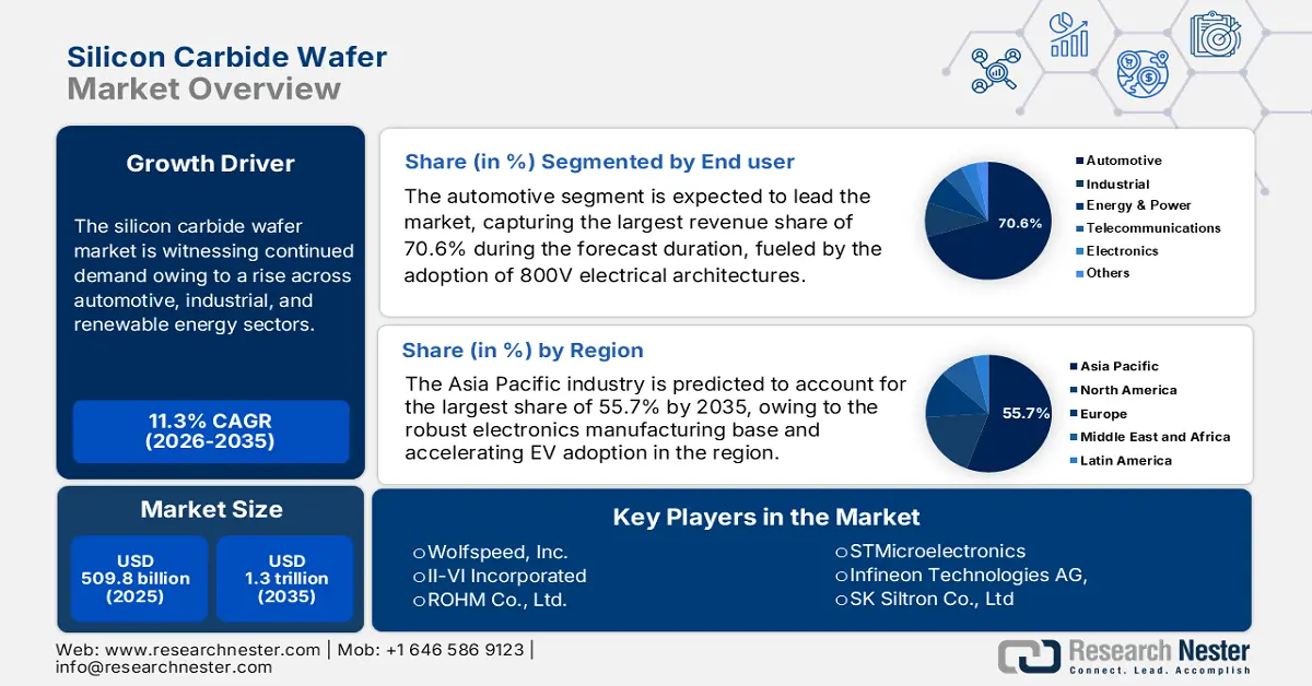
The silicon carbide wafer market is witnessing continued demand owing to a rise across automotive, industrial, and renewable energy sectors. Also, the transition toward electric vehicles, energy-efficient power systems, and high-voltage applications is driving manufacturers to expand production capacity. In December 2025, the article published by OECD found that the semiconductor value chain, which includes raw materials, wafer fabrication, and front-end semiconductor manufacturing, remains highly concentrated and interdependent, with a small number of countries supplying critical inputs. It notes that about 90% of global wafer‑fabrication capacity is located in just five economies: China, Taiwan, South Korea, Japan, and the U.S. Hence, this provides a strong, scalable infrastructure that can efficiently meet rising demand for SiC wafers.
Furthermore, in January 2024 U.S. Geological Survey, Mineral Commodity Summaries found that in 2023, U.S. silicon materials were produced at six facilities, primarily serving the steel, aluminum, chemical, semiconductor, and solar industries. The U.S. relies on imports for both ferrosilicon and silicon metal, with notable global supply arising from China, Brazil, Norway, and Russia. In addition, the worldwide production of silicon materials remained stable, wherein China was recognized as the major producer, which is producing over 70% of the total. Simultaneously, the ongoing U.S. investments, including new solar-grade wafer facilities, reflect efforts to expand domestic high-purity silicon production and reduce reliance on foreign sources. Hence, readily increasing domestic silicon production is strengthening the supply of high-purity silicon, supporting both growth and scalability of the silicon carbide (SiC) wafer market.
Key Silicon Carbide Wafer Market Insights Summary:
Regional Insights:
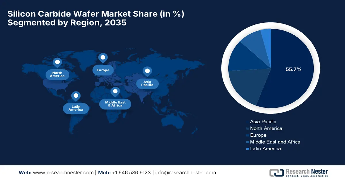
- Asia Pacific is projected to hold a 55.7% share by 2035, owing to its robust electronics manufacturing base and accelerating EV adoption.
- North America is expected to grow rapidly by 2035, driven by electrification in transportation and expanding domestic SiC fabrication capacity.
Segment Insights:
- Automotive subsegment is projected to account for 70.6% share by 2035, impelled by the rapid adoption of 800V electrical architectures.
- 150 mm wafer size subsegment is likely to capture significant market share by 2035, owing to the transition from 100 mm to 150 mm wafers reducing chip manufacturing costs.
Key Growth Trends:
- EV & power electronics demand
- Expansion of renewable energy and grid infrastructure applications
Major Challenges:
- High production costs
- Manufacturing complexity and yield issues
Key Players: II‑VI Incorporated (now Coherent Corp.) (U.S.), ROHM Co., Ltd. (Japan), STMicroelectronics (Switzerland), Infineon Technologies AG (Germany), SK Siltron Co., Ltd. (South Korea), Showa Denko K.K. (Japan), TankeBlue Semiconductor Co., Ltd. (China), SICC Co., Ltd. (Taiwan), Xiamen Powerway Advanced Material Co., Ltd. (China), Sumitomo Electric Industries, Ltd. (Japan), Hebei Synlight Crystal Co., Ltd. (China), Dow (DuPont) (U.S.), Entegris, Inc. (U.S.), Toshiba Corporation (Japan).
Global Silicon Carbide Wafer Market Forecast and Regional Outlook:
Market Size & Growth Projections:
- 2025 Market Size: USD 509.8 billion
- 2026 Market Size: USD 567.4 billion
- Projected Market Size: USD 1.3 trillion by 2035
- Growth Forecasts: 11.3% CAGR (2026-2035)
Key Regional Dynamics:
- Largest Region: Asia Pacific (55.7% Share by 2035)
- Fastest Growing Region: North America
- Dominating Countries: United States, China, Germany, Japan, United Kingdom
- Emerging Countries: India, Brazil, South Korea, Australia, Indonesia
Last updated on : 10 December, 2025
Silicon Carbide Wafer Market - Growth Drivers and Challenges
Growth Drivers
- EV & power electronics demand: The global shift towards electric mobility is the primary fueling factor for the expansion of the silicon carbide wafer market. These wafers are utilized in EV inverters, onboard chargers, and power‑electronics modules since they support higher voltages, offer better thermal performance. The article published by the U.S. Department of Energy in November 2024 reported that its Loan Programs Office highlighted the rising demand for advanced vehicle components, which include power electronics critical for EV efficiency and performance. Simultaneously, programs such as ATVM, LPO have supported domestic manufacturing of semiconductors and related components, wherein the financing requests totaled USD 16.8 billion as of mid-2024, demonstrating strong interest in onshoring advanced EV supply chains. Hence, this directly supports the adoption of high-efficiency power electronics, thereby driving consistent demand for silicon carbide wafers in EV inverters and modules.
- Expansion of renewable energy and grid infrastructure applications: The progress in terms of solar, wind, and energy‑storage installations, and the heightened demand for smarter power conversion in grids and industrial power systems, is prompting stronger adoption in the silicon carbide (SiC) wafer market. Oak Ridge National Laboratory and the National Renewable Energy Laboratory in December 2025 demonstrated SiC-based power electronics for photovoltaic inverters, stating that SiC can operate at higher voltages and temperatures with faster switching and reduced energy loss when compared to silicon. It also stated that SETO-funded projects are advancing SiC inverter and converter designs for grid integration, energy storage, and microgrids, whereas U.S. SiC is also being explored in concentrating solar power applications, including 3D-printed heat exchangers and stable solar receivers, highlighting its efficiency for renewable energy systems.
- Technological advances: This, coupled with wafer‑manufacturing scale‑improvements such as larger wafer diameters and efficient crystal growth, is lowering the cost per wafer, thereby improving yields and making these wafers more commercially viable at scale. In May 2023, Infineon Technologies AG announced that it had signed a strategic agreement with China-based SiC supplier SICC to diversify its silicon carbide material sources, securing high-quality 150 mm wafers and boules for SiC semiconductor production. The firm also stated that the collaboration will initially focus on 150 mm wafers but also support Infineon’s transition to 200 mm wafers, enhancing supply chain stability amid growing demand from automotive, solar, EV charging, and energy storage sectors, hence supporting the rapid growth of the silicon carbide wafer market.
Recent Developments in SiC Wafer Manufacturing and Investment
|
Year |
Company |
Event |
Market Focus |
Notes |
|
2024 |
TanKeBlue |
SEMICON China exhibition |
SiC wafer products |
Launch of 8-inch conductive Epi-wafer, expanded substrate & epitaxy portfolio. |
|
2023 |
DENSO |
Minority investment in Silicon Carbide LLC |
SiC wafer procurement |
USD 500 million for stable supply of 150mm & 200mm wafers, 12.5% stake |
Source: Company Official Press Releases
Challenges
- High production costs: This is a major obstacle for the SiC wafer market growth since they show up with more expensive production costs when compared to traditional silicon wafers. Also, the cost per wafer can be two to four times higher, influenced by the complexity of the raw material, crystal growth, slicing, and polishing processes, which in turn leads to higher device costs for both manufacturers and end-users. The presence of pricing concerns can limit adoption in cost-sensitive applications, particularly in emerging markets or low-margin sectors. In addition to scaling to larger wafer diameters, such as 200 mm, it necessitates substantial capital investment in specialized equipment and infrastructure. Furthermore, until yields improve and production processes are more efficient, high costs are considered to be a critical barrier to widespread adoption.
- Manufacturing complexity and yield issues: The silicon carbide (SiC) wafer market presents intricate manufacturing challenges due to the material’s hardness, high melting point, and propensity for crystal defects. In this context, producing high-quality, large-diameter wafers, i.e., 150 mm to 200 mm, without any dislocations, micropipes, or other defects, is difficult, leading to variable yields. Even very small defects can render wafers unusable for high-performance devices, which in turn increases waste and production costs. On the other hand, the epitaxial growth process, required for device-ready wafers, demands precise control over doping, thickness uniformity, and crystal quality. Since manufacturers push for larger wafer sizes, yield improvement is highly essential to ensure cost-effectiveness and maintain competitiveness in various applications.
Silicon Carbide Wafer Market Size and Forecast:
| Report Attribute | Details |
|---|---|
|
Base Year |
2025 |
|
Forecast Year |
2026-2035 |
|
CAGR |
11.3% |
|
Base Year Market Size (2025) |
USD 509.8 billion |
|
Forecast Year Market Size (2035) |
USD 1.3 trillion |
|
Regional Scope |
|
Silicon Carbide Wafer Market Segmentation:
End user Segment Analysis
The automotive subsegment based on end user is expected to lead the global SiC wafer market, capturing the largest revenue share of 70.6% during the forecast duration. This growth is fueled by the rapid adoption of 800V electrical architectures, which are essential for next-generation EVs. Also, these silicon carbide devices are highly essential for managing these higher voltages with lower losses. In May 2025, Nexperia announced that it had launched new AEC-Q101-qualified 1200 V silicon carbide MOSFETs in the compact D2PAK-7 package, which offers RDS(on) options of 30, 40, and 60 mΩ for high-efficiency in automotive applications. Besides, these devices possess exceptional thermal stability, with RDS (on) increasing only 38% from 25 °C to 175 °C, which also outperforms typical SiC solutions, thereby enabling higher output power, reduced cooling requirements, and overall lower system cost for EV chargers, traction inverters, and HVAC systems.
Wafer Size Segment Analysis
In the wafer size segment 150 nm subsegment is likely to attain a significant share in the silicon carbide (SiC) wafer market over the discussed timeframe. The shift from 100mm to 150mm wafers is a key industry driver for reducing chip manufacturing costs by increasing the number of dies per wafer, thus improving economies of scale. Also, this transition is highly essential to meet the booming demand from the automotive sector. In April 2024, ROHM announced that its SiCrystal and STMicroelectronics have expanded their long-term agreement for 150 mm silicon carbide (SiC) substrate wafers, securing additional volumes which were valued at a minimum of USD 230 million. This deal strengthens ST’s global supply chain as it scales SiC device production for automotive and industrial silicon carbide wafer markets, whereas SiCrystal continues to ramp manufacturing in Germany, hence denoting a wider segment scope.
Application Segment Analysis
By the conclusion of 2025, the electric vehicles in terms of application is expected to command a lucrative share in the silicon carbide wafer market. The global transition towards electric mobility, demanding high-voltage power electronics for superior efficacy, is the key factor behind this leadership. Also, silicon carbide enables this in traction inverters, onboard chargers, along DC-DC converters. In July 2025, onsemi announced that it had expanded its collaboration with Schaeffler through a new design win that integrates next-generation EliteSiC MOSFETs into a traction inverter for a major global automaker’s next-gen plug-in hybrid EV platform. The firm also mentioned that EliteSiC technology delivers lower conduction losses, superior thermal performance, and high power density, thereby enabling longer driving range, enhanced reliability, and more compact inverter designs.
Our in-depth analysis of the silicon carbide (SiC) wafer market includes the following segments:
|
Segment |
Subsegments |
|
End user |
|
|
Wafer Size |
|
|
Application |
|
|
Product |
|
|
Wafer Diameter |
|
|
Polishing Type |
|

Vishnu Nair
Head - Global Business DevelopmentCustomize this report to your requirements — connect with our consultant for personalized insights and options.
Silicon Carbide Wafer Market - Regional Analysis
APAC Market Insights
Asia Pacific is likely to capture the largest revenue share of 55.7% in the global SiC wafer market by the end of 2035. The dominance of the region in this field is effectively attributable to the robust electronics manufacturing base and accelerating EV adoption. The region is witnessing continuous investment in local wafer fabs and strong government backing, which ensures rapid technology diffusion across major sectors. In August 2025, Toshiba and SICC announced that they had signed an MOU to explore collaboration, which is aimed at improving the characteristics and quality of SICC’s silicon carbide power semiconductor wafers and strengthening stable wafer supply to Toshiba. This partnership supports Toshiba’s accelerated development of SiC devices for automotive, server power, and high-efficiency conversion systems, where reliability and performance are highly essential.
China is the key growth engine for the silicon carbide (SiC) wafer market in the region, which is efficiently backed by massive EV production, a fast-growing domestic semiconductor industry, and strong policy support for wide-bandgap technologies. On the other hand, companies are readily expanding SiC wafer, epi, and device manufacturing with a collective goal of strengthening supply independence and meeting rising demand from national EV and power infrastructure projects. STMicroelectronics and Sanan Optoelectronics announced in June 2023, announced that entered into a strategic alliance to form a joint venture in Chongqing to manufacture 200 mm silicon carbide power devices for the country’s growing electric vehicle and industrial energy sectors. The JV will produce SiC devices exclusively for ST using its proprietary process, whereas Sanan will separately build a dedicated 200 mm SiC substrate facility to supply the operation.
India is continuously growing in the silicon carbide wafer market owing to the strong push for EV adoption, grid modernization, and domestic semiconductor development. On the other hand, government-backed initiatives are drawing interest from global SiC players to make investments in the country, whereas domestic research institutions work to advance materials capabilities for future power electronics production. In August 2025, the country’s government announced that it had approved four new semiconductor manufacturing projects with a total investment of Rs. 4,600 crore (USD 552 million), thereby boosting India’s semiconductor ecosystem. The report also stated that SiCSem, in collaboration with Clas-SiC Wafer Fab, will set up India’s first commercial silicon carbide (SiC) compound semiconductor fab in Odisha, while CDIL expands its SiC device production in Punjab. Furthermore, additional projects include advanced packaging by 3D Glass Solutions in Odisha and ASIP Technologies in Andhra Pradesh, hence denoting a silicon carbide wafer market outlook.
North America Market Insights
North America is expected to grow at a rapid pace in the silicon carbide (SiC) wafer market, driven by rapid electrification in transportation, strong investment in EV power electronics, and expanding domestic SiC fabrication capacity. The region also benefits from partnerships between automakers and semiconductor suppliers that are accelerating adoption, whereas government initiatives supporting clean energy and reshoring are boosting domestic SiC ecosystem growth. In July 2023, Renesas and Wolfspeed announced that they had signed a 10-year silicon carbide wafer supply agreement, with Renesas providing a USD 2 billion deposit to secure both 150mm and 200mm wafers, supporting Wolfspeed’s U.S. capacity expansion. Also, the agreement enables Renesas to scale production of SiC power semiconductors, meeting rising demand in automotive, industrial, and energy markets.
In the silicon carbide wafer market, the U.S. has gained immense exposure propelled by the presence of a well-established semiconductor supply chain, research programs, and significant expansion by major SiC producers. Simultaneously, EV manufacturers and renewable energy projects are relying on the country’s SiC capacity by maintaining competitiveness in this field. Coherent Corp. in December 2025, introduced a next-generation 300mm silicon carbide platform, which is aimed at enhancing thermal efficiency for AI datacenter infrastructure, building on its expertise with 200mm substrates. Also, these larger wafers offer improved power density, low resistivity, and high thermal stability, which support applications in datacenters, AR/VR devices, and power electronics. Hence, this advancement positions Coherent as a predominant leader in wide-bandgap semiconductors and demonstrates its commitment to scalable solutions for computing and renewable energy sectors.
Canada is growing exponentially in the SiC wafer market through its focus on sustainable mobility and clean energy, supported by EV assembly growth and regional innovation hubs. Simultaneously, collaborations between industry and academia are efficiently enhancing materials research, creating encouraging opportunities for SiC technologies in transportation, power grids, and industrial electrification. Besides, the country’s market also benefits from government initiatives and funding programs, which are efficiently strengthening the semiconductor ecosystem, providing resources for advanced materials and wafer fabrication research. Key players in the private sector are investing in SiC production capabilities and partnerships with international leaders to secure long-term supply chains. Furthermore, this combined approach positions Canada as a rising hub for silicon carbide wafer innovation, thereby contributing to global adoption in electric vehicles, renewable energy, and high-efficiency power electronics.
Europe Market Insights
Europe has acquired the most prominent position in the international silicon carbide wafer market owing to its leadership in automotive electrification and stringent energy-efficiency policies. Regional supply chains are strengthening since both the established and emerging entities in the region are making investments in SiC wafer and device production to support next-generation EV platforms. GF Machining Solutions in January 2025 announced the launch of the LASER S 500 U, which is a laser ablation machine especially designed for silicon carbide wafer manufacturing. The company also stated that the LASER S 500 U transforms this process with non-contact laser technology, reducing processing times from hours to minutes, thereby eliminating tool wear and lowering costs. Furthermore, it is coupled with GF’s LaserSUITE360 software and enables precise edge profiles, notch shapes, and wafer resizing, while embedded cameras ensure accurate identification and handling.
Germany is considered to be the dominating country in the regional SiC wafer market, driven by major automakers transitioning to SiC-based power systems. The country also leverages strong engineering expertise and strong investments in wafer and device technologies to support the leadership in high-performance EV and industrial power applications. In this regard, AIXTRON SE in September 2025 announced that it has shipped its 100th G10-SiC system, which marks a significant milestone in the global adoption of its SiC epitaxy batch technology. This G10-SiC system supports high-volume production of 150 mm and 200 mm silicon carbide wafers, which are essential for efficient power devices used in electric vehicles, renewable energy, and industrial power supplies. Furthermore, it has a multi-wafer 6×200 mm configuration and Multi-Ject technology, which allows it to deliver uniform, high-quality epitaxial layers, enabling scalable, high-throughput manufacturing.
The U.K. is also maintaining a stronger position in the regional silicon carbide wafer market through R&D-focused initiatives that support SiC materials development and power electronics innovation. Collaboration between major industrial leaders is encouraging progress in SiC wafer technologies for EV prototypes, aerospace electrification, and next-generation energy systems. Clas-SiC Wafer Fab Limited, in October 2024, reported that it successfully achieved a GBP 15 million ( ≈ USD 18.75 million) investment that will be utilized to expand its manufacturing capabilities and advance its technology development. The company also notes that this investment aims to strengthen its position in the semiconductor industry, which is focused on energy-efficient SiC devices. Hence, this aspect of commitment to build an efficient ecosystem highlights its role in supporting the worldwide transition to electrification and sustainable technologies in the years ahead.
Key Silicon Carbide Wafer Market Players:
- Wolfspeed, Inc. (U.S.)
- Company Overview
- Business Strategy
- Key Product Offerings
- Financial Performance
- Key Performance Indicators
- Risk Analysis
- Recent Development
- Regional Presence
- SWOT Analysis
- II‑VI Incorporated (now Coherent Corp.) (U.S.)
- ROHM Co., Ltd. (Japan)
- STMicroelectronics (Switzerland)
- Infineon Technologies AG (Germany)
- SK Siltron Co., Ltd. (South Korea)
- Showa Denko K.K. (Japan)
- TankeBlue Semiconductor Co., Ltd. (China)
- SICC Co., Ltd. (Taiwan)
- Xiamen Powerway Advanced Material Co., Ltd. (China)
- Sumitomo Electric Industries, Ltd. (Japan)
- Hebei Synlight Crystal Co., Ltd. (China)
- Dow (DuPont) (U.S.)
- Entegris, Inc. (U.S.)
- Toshiba Corporation (Japan)
- Wolfspeed, Inc. is widely regarded as a leading pioneer in SiC materials and wafers, with end-to-end capabilities from crystal growth to finished substrates and even power‑device fabrication. It operates one of the world’s first and largest 8-inch (200 mm) SiC wafer fabrication plants, a major advantage when scaling production for high‑power and automotive applications. Its combination of technological leadership, vertical integration, and large-scale capacity gives Wolfspeed a strong competitive position, especially for high-volume SiC wafers destined for EVs, renewable‑energy, and industrial power electronics.
- II‑VI Incorporated, now more commonly referred to as Coherent Corp., is a major global supplier of engineered materials, including SiC substrates and epitaxial wafers for power electronics and RF applications. The company has leveraged its advanced crystal‑growth and wafering capabilities to serve a broad set of end‑users. Further, since the demand for SiC is increasing for EV, industrial, and energy sectors, II-VI’s diversified product portfolio and manufacturing expertise give it a competitive foothold.
- ROHM Co., Ltd., often through its SiC-focused subsidiary SiCrystal GmbH, is also another heavyweight in this field. The company has a well-established presence in both substrate/wafer production and power‑device manufacturing, enabling a vertically integrated “wafer-to-device” supply chain. ROHM emphasizes notable investments and a strong focus on automotive and industrial applications, especially for silicon carbide wafer markets that are witnessing high reliability and mass-managed quality control.
- STMicroelectronics N.V. is also well recognized among the leading companies since it has broad semiconductor manufacturing capabilities. The company combines wafer supply with device fabrication, enabling it to serve automotive, industrial, and renewable‑energy clients with integrated SiC-based solutions. Furthermore, the company has a diversified footprint and global customer base, which gives it flexibility and resilience as the market expands and demand becomes more geographically dispersed.
- Infineon Technologies AG has emerged as the most prominent contender in the SiC wafer landscape, particularly after recent milestones in its 200 mm SiC wafer roadmap. The company has integrated SiC wafer supply with its power‑semiconductor device production by leveraging wafer-to-module vertical integration to offer high-voltage, high-efficiency SiC solutions for EVs, renewable energy systems, and industrial power electronics. Furthermore, Infineon’s position as a global semiconductor leader gives it strong market reach and the capacity to respond to increasing SiC demand.
Below is the list of some prominent players operating in the global SiC wafer market:
The pioneers, such as Wolfspeed, Coherent, ROHM, STMicroelectronics, and Infineon, are dominating the silicon carbide wafer market with their extensive substrate supply and also often produce power devices. These companies are making investments in capacity expansion, upgrading to 8-inch or 200 mm wafer lines, scaling the epitaxial quality, and reinforcing their supply‑chain control to meet heightened demand from various sectors. In September 2024, Coherent Corp. announced that it had launched 200 mm silicon carbide (SiC) epitaxial wafers having 350 µm and 500 µm thickness, which marks a major advancement in high-quality, uniform SiC substrate production. The firm also notes that this larger wafer size enables manufacturers to produce more devices per wafer, improving yield, and thereby supporting high-performance SiC power semiconductors for EVs, energy infrastructure, and high-power chargers supporting long-term silicon carbide wafer market expansion.
Corporate Landscape of the SiC wafer market:
Recent Developments
- In December 2025, X-FAB announced the launch of its XbloX platform, which offers a scalable and standardized SiC process technology to accelerate the development and production of advanced power MOSFETs.
- In September 2025, Wolfspeed, Inc. announced the launch of its 200mm silicon carbide (SiC) materials portfolio, which includes bare wafers and epitaxy, marking a major step in scaling high-performance power device production.
- In February 2025, Infineon Technologies declared that it began rolling out its first products based on 200 mm silicon carbide (SiC) wafer technology from its Villach, Austria, facility, targeting high-voltage applications such as EVs, renewable energy, and trains.
- In June 2024, onsemi announced plans to establish a vertically integrated silicon carbide manufacturing facility in the Czech Republic with a multi-year investment of up to USD 2 billion to produce advanced power semiconductors for various applications.
- Report ID: 8302
- Published Date: Dec 10, 2025
- Report Format: PDF, PPT
- Explore a preview of key market trends and insights
- Review sample data tables and segment breakdowns
- Experience the quality of our visual data representations
- Evaluate our report structure and research methodology
- Get a glimpse of competitive landscape analysis
- Understand how regional forecasts are presented
- Assess the depth of company profiling and benchmarking
- Preview how actionable insights can support your strategy
Explore real data and analysis
Frequently Asked Questions (FAQ)
Silicon Carbide Wafer Market Report Scope
Free Sample includes current and historical market size, growth trends, regional charts & tables, company profiles, segment-wise forecasts, and more.
Connect with our Expert


Copyright @ 2026 Research Nester. All Rights Reserved.
