Through-Silicon Via (TSV) Technology Market Outlook:
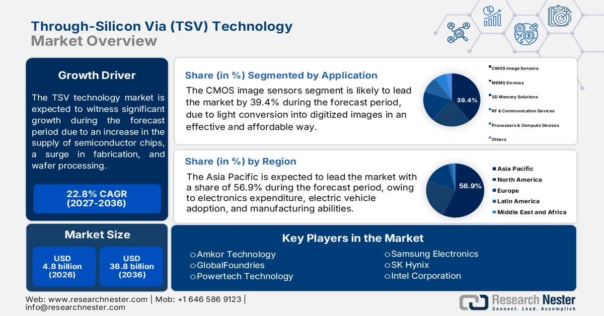
Through-Silicon Via Technology Market size was valued at USD 4.8 billion in 2026 and is projected to exceed USD 36.8 billion by the end of 2036, expanding at over 22.8% CAGR during the forecast period, i.e., 2027-2036. In 2027, the industry size of through-silicon via technology is assessed at USD 5.8 billion.
The worldwide through-silicon via technology market is shaped by an interplay of factors, such as high-density TSV fabrication, thermal management constraints in stacked GPU modules, and supply chain dynamics for specialty equipment for bonding, lithography, and wafer-based processing. According to an article published by the OECD in December 2025, 5 economies, including the U.S., Japan, Korea, Taipei, and China, together account for 87% of global in-production wafer capacity. Based on this, the wafer capacity in Korea is effectively focused, with nearly 80% of its capacity originating from Samsung and SK Hynix, heavily investing in memory chip production. Besides, DRAM and NAND production highly depends on process nodes that usually range from 6 nm to more than 22 nm, thereby making it suitable for positively impacting the market’s growth and exposure.
Number of Companies Across 5 Economies Generating Wafer Capacity, 2024
|
Country Name |
Number of Companies |
|
China |
181 |
|
Taiwan |
46 |
|
Korea |
22 |
|
Japan |
73 |
|
U.S. |
155 |
|
Singapore |
15 |
|
Germany |
31 |
|
Malaysia |
7 |
|
Austria |
3 |
Source: OECD
Furthermore, the shift to thermal-aware TSV design, along with the integration of hybrid and fine-pitch bonding, and regionalization of semiconductor manufacturing, are a few trends that are responsible for positively boosting the through-silicon via technology market globally. As stated in an article published by the Semiconductor Industry Association (SIA) in July 2026, the worldwide semiconductor sales effectively reached a record USD 795.6 billion as of 2025. This eventually surpassed the World Semiconductor Trade Statistics (WSTS) organization’s projection of USD 1.5 trillion as of 2026. Therefore, this rapid growth reflected the escalating deployment of artificial intelligence (AI) and the ongoing expansion of innovative computing, emerging 6G and 5G communications. Additionally, this particular growth also positively catered to innovations in advanced defense systems, healthcare devices, and other semiconductor-based advancements.
Key Through-Silicon Via (TSV) Technology Market Insights Summary:
Regional Highlights:
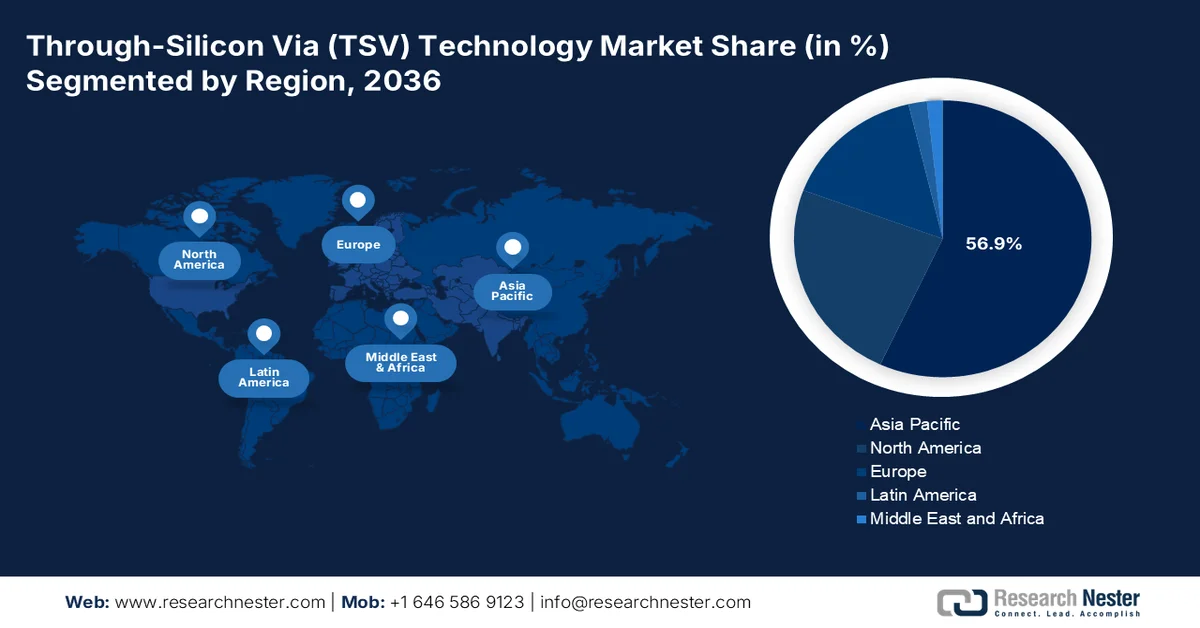
- Asia Pacific is projected to command the largest 56.9% share of the through-silicon via (TSV) technology market by 2036, supported by extensive manufacturing capabilities, expanding electronics spending, and rapid deployment of autonomous vehicles
- Europe is anticipated to register the fastest growth during the forecast period, capturing a 15.6% share, propelled by semiconductor innovation, advanced driver assistance systems, and a strong industrial focus on automotive electrification
Segment Insights:
- The CMOS image sensors sub-segment is forecast to secure the largest 39.4% share of the through-silicon via (TSV) technology market by 2036, driven by its efficient, high-speed conversion of light into digital images across smartphones, automotive systems, and medical applications
- The medium diameter TSV (5-10 µm) sub-segment is expected to capture a suitable share during the forecast period, owing to its balance between interconnect density and manufacturing feasibility across memory solutions, processors, and compute devices
Key Growth Trends:
- Demand for AI and high-bandwidth memory
- Miniaturization across edge and imaging devices
Major Challenges:
- Manufacturing complexity and yield constraints
- Material and equipment supply chain vulnerabilities
Key Players: Samsung Electronics (South Korea),Taiwan Semiconductor Manufacturing Company Limited (TSMC) (Taiwan),SK Hynix (South Korea),Intel Corporation (U.S.),ASE Group (Taiwan),Amkor Technology (U.S.),GlobalFoundries (U.S.),Powertech Technology (Taiwan).
Global Through-Silicon Via (TSV) Technology Market Forecast and Regional Outlook:
Market Size & Growth Projections:
- 2026 Market Size: USD 4.8 billion
- 2027 Market Size: USD 5.8 billion
- Projected Market Size: USD 36.8 billion by 2036
- Growth Forecasts: 22.8% CAGR (2027-2036)
Key Regional Dynamics:
- Largest Region: Asia Pacific (56.9% share by 2036)
- Fastest Growing Region: Europe
- Dominating Countries: China, Taiwan, South Korea, Japan, United States
- Emerging Countries: Singapore, India, Germany, France, Netherlands
Last updated on : 9 September, 2026
Through-Silicon Via (TSV) Technology Market - Growth Drivers and Challenges
Growth Drivers
- Demand for AI and high-bandwidth memory: The workload of memory bandwidth that is necessary for AI interface and training is considered a suitable growth driver for the through-silicon via technology market globally. According to an article published by the Federal Reserve Board in February 2026, there has been an increase in AI-based investment that has been effectively driven by robust growth, with over USD 272 billion in trade in 2024, which indicated a 65% surge in the first half of 2024. Besides, AI imports have also more than doubled, with strong growth and a huge increase in imports as of 2025, owing to frontloading. Meanwhile, China and the U.S. significantly drove growth in AI imports, with the U.S. escalating further growth, followed by initial increase in China-based imports, thus proliferating the market upliftment.
- Miniaturization across edge and imaging devices: The push for miniaturization across imaging and edge devices continues to drive the through-silicon via technology market adoption, as smartphones, automotive cameras, medical instruments, wearables, and industrial sensors demand increasingly compact yet feature-rich modules. Additionally, TSV technology enables vertical rerouting of electrical connections within image sensors and stacked components, eliminating the need for expansive surface-area interconnects and allowing significantly thinner package profiles. This capability is translating into tangible market outcomes, with wafer-level packaging companies securing more design wins and achieving greater product differentiation in camera and sensor modules.
Challenges
- Manufacturing complexity and yield constraints: The fabrication of high-aspect-ratio TSVs with ultra-fine pitches introduces significant process control challenges. Etching deep, narrow vias through silicon wafers demands exceptional precision, while subsequent copper filling must be void-free to ensure electrical reliability. Even minor deviations in etch uniformity or plating consistency can result in latent defects that only manifest during thermal cycling, reducing overall production yields. The strain induced by TSV fabrication can also shift transistor thresholds in adjacent active regions, forcing conservative design rules that consume valuable silicon area. These compounding technical hurdles create limitations in the market growth.
- Material and equipment supply chain vulnerabilities: The through-silicon via technology market manufacturing ecosystem depends heavily on specialized equipment and advanced materials that are concentrated among a limited number of global suppliers. Lithography tools, bonding systems, and wafer-level processing equipment face geographical concentration, creating exposure to regional disruptions. Export control regimes and trade restrictions further constrain access to these critical technologies in certain markets, limiting capacity expansion and regional participation. Additionally, the supply of high-purity copper, dielectric materials, and barrier layers remains vulnerable to fluctuations in raw material availability.
Through-Silicon Via (TSV) Technology Market Size and Forecast:
| Report Attribute | Details |
|---|---|
|
Base Year |
2026 |
|
Forecast Year |
2027-2036 |
|
CAGR |
22.8% |
|
Base Year Market Size (2026) |
USD 4.8 billion |
|
Forecast Year Market Size (2036) |
USD 36.8 billion |
|
Regional Scope |
|
Through-Silicon Via (TSV) Technology Market Segmentation:
Application Segment Analysis
Based on the application segment, the CMOS image sensors sub-segment is anticipated to grab the largest share of 39.4% in the through-silicon via technology market by the end of 2036. The sub-segment’s upliftment is primarily fueled by its importance for converting light into digital images in a cost-effective and efficient way at high speeds, powering from regular smartphones to innovative automotive and medical systems. According to an article published by MDPI in November 2023, these image sensors usually comprise 2.7 µm and 0.5 MP pixels that are effectively packed in a die size of 2.3 mm × 2.8 mm. Based on this, the sensor type is focused on achieving more than 93% quantum efficiency, particularly in the visible wavelength and over 36% in near-infrared, while effectively drawing 20 mW at a 10-bit. Therefore, based on all these aspects, there is a huge growth opportunity for the sub-segment’s growth.
Diameter Segment Analysis
During the forecast period, the medium diameter TSV (5-10 µm) sub-segment under the diameter segment is predicted to account for a suitable share in the market. The sub-segment’s growth is effectively driven by representing the most versatile and widely adopted via size range across the semiconductor industry. These vias strike an optimal balance between interconnect density and manufacturing feasibility, making them suitable for a broad spectrum of applications including memory solutions, processors, and compute devices. The aspect ratios achievable within this diameter range allow for reliable copper filling while maintaining acceptable yield levels. Besides, medium-diameter vias accommodate the performance requirements of high-bandwidth memory stacks and advanced logic integration without pushing process capabilities to their limits.
End use Industry Segment Analysis
The foundries segment, which is part of the end use industry, is expected to garner a considerable share in the market by the end of the stipulated timeline. The segment’s development is highly propelled by serving as manufacturing hubs for fabless semiconductor companies and IDMs alike. These facilities integrate TSV processes into their advanced node offerings, enabling customers to access 3D stacking capabilities without substantial capital investment. Additionally, foundries typically adopt via-middle approaches to maintain compatibility with high-performance CMOS logic flows. Their role extends beyond mere fabrication, as they provide design enablement tools and process design kits that facilitate TSV implementation. The concentration of TSV capacity within foundries reflects their strategic position in enabling widespread adoption of 3D integration technologies across diverse semiconductor applications.
Our in-depth analysis of the through-silicon via technology includes the following segments:
|
Segment |
Subsegments |
|
Application |
|
|
Diameter |
|
|
End use Industry |
|
|
Process Type |
|

Vishnu Nair
Head - Global Business DevelopmentCustomize this report to your requirements — connect with our consultant for personalized insights and options.
Through-Silicon Via (TSV) Technology Market - Regional Analysis
APAC Market Insights
The Asia Pacific through-silicon via technology market is anticipated to grab the highest share of 56.9% by the end of 2036. The market’s upliftment in the region is primarily attributed to massive manufacturing capabilities, an expansion in electronics spending, and the rapid deployment of autonomous vehicles. According to a data report published by WITS in 2021, the export of semiconductor devices in China amounted to USD 434,183.9 in trade valuation and a shipment of 6,609,660,000 items. Likewise, the export of such devices also amounted to USD 428,028.7 in trade and 798,484,000 items in quantity in Singapore. Meanwhile, Japan constitutes USD 133,445.1, along with 928,523,000 items in quantities, while it is USD 13,141,2 and 4,948,670 in India, thereby making it suitable for creating an optimistic outlook for the market in the region.
The through-silicon via technology market in China is growing significantly, owing to governmental investment in domestic packaging and semiconductor capabilities, an upsurge in data center infrastructure, electric vehicles, and consumer electronics. As per a data report published by the OEC in 2024, the export of electric motor vehicles in the country accounted for USD 32.7 billion, while the import valuation amounted to USD 795 million. Besides, according to the July 2025 Center for Strategic and International Studies (CSIS) article, there are continuously growing exports of national internal combustion engine vehicles, which are eventually increasing across every region and also readily challenging the conventional automotive production in emerging economies. Therefore, the sales share of electric vehicles in the country also increased, thus positively impacting the market growth.
Electric Vehicle Sales Share in China, 2015-2025
|
Year |
Share % |
|
2015 |
0.8 |
|
2016 |
1.5 |
|
2017 |
2.4 |
|
2018 |
4.5 |
|
2019 |
5.0 |
|
2020 |
5.7 |
|
2021 |
13.9 |
|
2022 |
26.7 |
|
2023 |
33.8 |
|
2024 |
44.3 |
|
2025 |
50.1 |
Source: CSIS
The aspects of semiconductor fabrication, organizational joint ventures and partnerships, generous investments, and growth in electronics manufacturing are certain factors that are boosting the through-silicon via technology market in India. As stated in an article published by the IBEF Organization in August 2026, the electronic manufacturing sector in the country grew by USD 40 billion to USD 45 billion as of 2025, which is further set to surpass USD 150 billion by the end of 2030. In addition, revenues in the industry accounted for almost 24% as of 2024 and are also estimated to grow nearly 27% by the end of 2029. Moreover, the sector also witnessed a 4-fold growth in 2025, wherein there was an increase in manufacturing from USD 31 billion to USD 130 billion. Besides, India makes up about 5% to 6% of the overall electronics manufacturing, thus positively enhancing the market’s demand.
Europe Market Insights
Europe market is expected to emerge as the fastest-growing region with a share of 15.6% during the forecast period. The market’s development in the region is highly propelled by innovation in semiconductors, innovative driver assistance systems, and a robust industrial focus on automotive electrification. According to an article published by the European Automobile Manufacturers’ Association (ACEA) in September 2026, the overall public charging capacity has effectively reached 41.6 GW as of June 2026, demonstrating an increase of 29%. Meanwhile, the number of public charging stations also surged by 21% year-on-year (YoY) to approximately 195,082 as of May 2026. Therefore, based on this growth, the region’s electric vehicle transition continued to develop, due to which the market’s demand is continuously increasing.
The through-silicon via technology market in Germany is gaining increased traction, owing to the sustained growing demand for 3D integration solutions, along with increased expansion in industrial and automotive manufacturing. As stated in a data report published by ITA in August 2025, 77% of national advanced manufacturing organizations are predicted to witness growth in the domestic market in the upcoming 24 months. Besides, the country’s industrial associations tend to cover measuring and sensor technology, based on which the VDMA’s Measuring and Testing Technology effectively comprises nearly 200 member organizations. Additionally, the automation industry division Measurement Technology and Process Automation significantly counts almost 100 member firms, thereby positively contributing to the market’s growth and demand in the overall nation.
The robust focus on high-performance computing, telecommunications infrastructure, and AI research facilities, as well as a supportive policy environment for innovative packaging, is highly responsible for driving the through-silicon via technology market in the UK. As per an article published by the UK Government in April 2026, more than 87% of national premises have access to a gigabit-based connection, and the government is focused on expanding by 99% by the end of 2032. Likewise, 4G connectivity across 95% of the country’s landmass is focusing on ensuring businesses and communities benefit from suitable connectivity. Besides, the nation’s ambition is also to comprise high-quality and standalone 5G services across all populated areas in the nation by the end of 2030. Therefore, with such governmental objectives to increase and extend telecom services, there is a huge demand for the market in the country.
North America Market Insights
North America market is predicted to account for a considerable share of 23.8% by the end of the stipulated timeline. The market’s growth in the region is effectively fueled by the provision of generous research and development investments, the demand for AI escalators in hyperscale data centers, and the presence of notable semiconductor organizations. According to an article published by Congress Government in May 2026, the U.S.-based data center yearly energy utilization as of 2023 effectively accounted for an estimated 176 terawatt-hours. This eventually caters to roughly 4.4% of the U.S. annual electricity consumption within the same year. Besides, hyperscale data centers have been developed with capacities from 100 MW to 1,000 MW each, which is almost equivalent to the load from 80,000 to 800,000 homes, thus positively driving the market’s upliftment in the region.
The market in the U.S. is gaining increased exposure, owing to massive government investment, a surge in AI facility demand, an expansion in major capacities, and the existence of a strong semiconductor research and development ecosystem. As stated in an article published by the Federal Reserve Government in April 2026, 18% of companies in the country have significantly integrated AI as of 2025. In addition, this adoption rate continued to grow by 68% by the end of September. Based on this growth, 78% of the domestic labor force operates at firms that have readily adopted AI, while 54% operates at firms that utilize large language models. Therefore, based on this continuous adoption, the market in the country is gradually and increasingly gaining increased importance.
The focus on niche technologies and the provision of generous government funding for semiconductor research and development are significantly responsible for bolstering the market in Canada. As per an article published by the Government of Canada in July 2024, the Minister of Innovation, Science and Industry offered a significant investment of USD 120 million in a more than USD 220 million project, which is led by CMC Microsystems. This particular investment, which has been made through the Strategic Innovation Fund, is focused on supporting the development of a domestic network by bringing together stakeholders. The ultimate purpose was to support the designing, manufacturing, and commercialization of semiconductors, along with the creation of state-of-the-art intelligent sensor technology, thus bolstering the market’s growth in the country.
Key Through-Silicon Via (TSV) Technology Market Players:
- Samsung Electronics (South Korea)
- Taiwan Semiconductor Manufacturing Company Limited (TSMC) (Taiwan)
- SK Hynix (South Korea)
- Intel Corporation (U.S.)
- ASE Group (Taiwan)
- Amkor Technology (U.S.)
- GlobalFoundries (U.S.)
- Powertech Technology (Taiwan)
- Company Overview
- Business Strategy
- Key Product Offerings
- Financial Performance
- Key Performance Indicators
- Risk Analysis
- Recent Development
- Regional Presence
- Samsung Electronics leverages its vertically integrated semiconductor business to deploy TSV technology across high-bandwidth memory stacks and advanced logic packages. The company's TSV capabilities are central to its memory-logic integration strategy, serving both internal product lines and external foundry clients.
- Taiwan Semiconductor Manufacturing Company Limited (TSMC) integrates TSV technology within its advanced packaging platforms to enable chiplet-based architectures and high-performance computing solutions. The company's approach to TSV implementation focuses on compatibility with leading-edge logic processes, serving fabless clients across compute and mobile segments.
- SK Hynix positions TSV technology as the foundational enabler for its high-bandwidth memory products targeting AI accelerators and data center applications. The company continues to refine its TSV processes to support increasing memory stack heights and bandwidth requirements.
- Intel Corporation employs TSV technology across its 3D stacking solutions, enabling heterogeneous integration of logic and memory within advanced processor packages. The company's TSV capabilities are embedded within its broader packaging roadmap, supporting both internal microprocessor development and foundry services.
- ASE Group offers TSV-based packaging services to fabless semiconductor companies, providing turnkey solutions for 2.5D and 3D integration requirements. The company's TSV capabilities span interposer fabrication, die stacking, and assembly for a diverse range of end-market applications.
Here is a list of key players operating in the global market:
The competitive landscape for the global through-silicon via technology market is moderately consolidated, with leading players leveraging distinct strategic advantages to secure their positions. Meanwhile, IDMs and foundries such as Samsung, TSMC, Intel, and SK Hynix dominate through vertical integration, combining in-house manufacturing with advanced packaging solutions for end-market products, such as high-bandwidth memory (HBM) and processors. Besides, in June 2025, Thin Film Interconnect strategically partnered with Heisler Semiconductor LLC, which combined technical strengths of 2 Maryland-specific advancements and delivered an end-to-end and complete solution for wafer production, thus positively impacting the TSV technology industry’s growth.
Corporate Landscape of the Market:
Recent Developments
- In July 2026, Intel Corporation and Lens Technology enabled a strategic collaboration and developed new technologies for innovative semiconductor packaging, and further explored opportunities to escalate the development of glass substrate-specific packaging solutions.
- In March 2026, STMicroelectronics entered high-volume production for its state-of-the-art silicon photonics-based PIC100 platform, which is readily utilized by hyperscalers for optical interconnect for AI clusters and data centers.
- Report ID: 8760
- Published Date: Sep 09, 2026
- Report Format: PDF, PPT
- Explore a preview of key market trends and insights
- Review sample data tables and segment breakdowns
- Experience the quality of our visual data representations
- Evaluate our report structure and research methodology
- Get a glimpse of competitive landscape analysis
- Understand how regional forecasts are presented
- Assess the depth of company profiling and benchmarking
- Preview how actionable insights can support your strategy
Explore real data and analysis
Frequently Asked Questions (FAQ)
About this Report
Connect with our Expert


Report, 2027-2036


Copyright @ 2026 Research Nester. All Rights Reserved.
