Chiplet Packaging Market Outlook:
Chiplet Packaging Market size was valued at USD 8.4 billion in 2025 and is projected to reach USD 30.4 billion by the end of 2035, registering around 13.7% CAGR during the forecast period, i.e., 2026-2035. In 2026, the industry size of chiplet packaging is estimated at USD 9.6 billion.
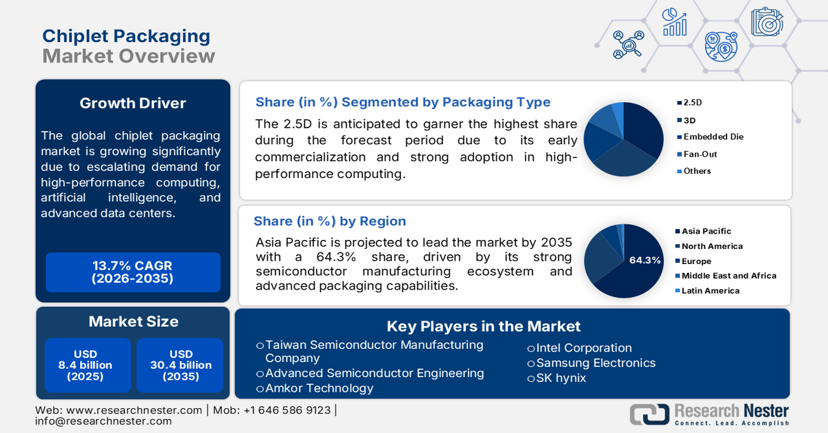
The global chiplet packaging market is experiencing immense growth, which is driven by the escalating demand for high-performance computing, artificial intelligence, and advanced data centers. The traditional monolithic semiconductor scaling faces physical and economic limitations, due to which chiplet architecture has emerged as a critical alternative, allowing smaller, specialized dies to be integrated into a single package. In October 2024, the Biden-Harris Administration announced a generous funding opportunity of up to USD 1.6 billion under the CHIPS and Science Act to advance U.S. semiconductor advanced packaging technologies. This initiative aims to strengthen domestic semiconductor packaging capabilities through R&D investments in areas such as chiplet ecosystems, thermal management, connector technologies, and packaging processes, thus positively benefiting the market’s expansion.
Furthermore, key technological innovations in advanced packaging, such as silicon interposers, embedded multi-die interconnect bridges, and vertical 3D stacking, are paving the way for unprecedented transistor density and faster interconnect speeds. Therefore, major semiconductor foundries and outsourced semiconductor assembly and test providers are aggressively expanding their advanced packaging capacities to capture this rapidly evolving market. In September 2023, Intel announced the advancement of the chiplet packaging through its innovative EMIB and Foveros advanced packaging technologies, which enable 2D and 3D heterogeneous integration of multiple chips within a single package. The company leverages advanced packaging to extend Moore’s Law, improve performance, and support next-generation computing applications.
Key Chiplet Packaging Market Insights Summary:
Regional Highlights:
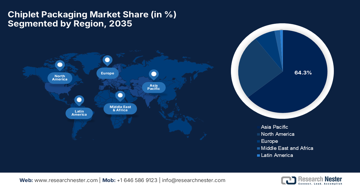
- The Asia Pacific region is projected to capture 64.3% of the chiplet packaging market by 2035, bolstered by its strong semiconductor manufacturing ecosystem, government-backed localization initiatives, substantial capital investments, and highly skilled workforce
- North America is poised for transformative growth throughout 2026-2035, supported by the accelerating push to strengthen domestic semiconductor supply chains and reshore advanced manufacturing capabilities
Segment Insights:
- The 2.5D segment is projected to account for the largest share of the chiplet packaging market by 2035, reinforced by its early commercialization and widespread adoption across high-performance computing, AI accelerators, graphics processors, and data-center applications, fueled by its ability to deliver high bandwidth, enhanced power efficiency, and scalable heterogeneous integration over conventional monolithic chip designs
- The Data Center segment is anticipated to witness considerable growth by 2035, underpinned by the increasing deployment of AI accelerator chips and advanced data-center processors
Key Growth Trends:
- Stagnation of Moore’s law
- Demand for high-performance computing
Major Challenges:
- Thermal management and reliability concerns
- Supply chain and ecosystem coordination challenges
Key Players: Taiwan Semiconductor Manufacturing Company, Advanced Semiconductor Engineering (ASE), Amkor Technology, Intel Corporation, Samsung Electronics, SK hynix, Silicon Box, Ares, Powertech Technology Inc. (PTI), Hanmi Semiconductor.
Global Chiplet Packaging Market Forecast and Regional Outlook:
Market Size & Growth Projections:
- 2025 Market Size: USD 8.4 billion
- 2026 Market Size: USD 9.6 billion
- Projected Market Size: USD 30.4 billion by 2035
- Growth Forecasts: 13.7% CAGR (2026-2035)
Key Regional Dynamics
- Largest Region: Asia Pacific (64.3% share by 2035)
- Fastest Growing Region: North America
- Dominating Countries: Taiwan, United States, China, South Korea, Japan
- Emerging Countries: India, Germany, Singapore, Vietnam, Italy
Last updated on : 23 July, 2026
Chiplet Packaging Market - Growth Drivers and Challenges
Growth Drivers
- Stagnation of Moore’s law: Traditional monolithic chip design faces intense physical and economic limits as scaling down transistors becomes difficult and costly. In this context, chiplet packaging provides an alternative pathway by breaking large dies into smaller, specialized pieces, which sustains performance gains. In May 2024, AMD reported that it was recognized with the IEEE 2024 corporate innovation award for its leadership in developing and deploying chiplet architectures for high-performance and adaptive computing. This company pioneered scalable chiplet-based designs across Ryzen CPUs, EPYC processors, and Instinct accelerators, improving performance, efficiency, and flexibility, thus benefiting the overall chiplet packaging market.
- Demand for high-performance computing: There has been a strong surge of AI, ML, and massive data centers, which require unprecedented processing power that can be provided by chiplet packaging, thereby allowing companies to mix and match processing units, memory, and accelerators on a single substrate. This customization delivers the high throughput and low latency that are needed for heavy computational workloads. In this context, NVIDIA in March 2024 introduced the Blackwell platform, which consists of a next-generation GPU architecture with advanced chip-to-chip interconnect technology that supports trillion-parameter AI models. It was built using a dual-die design connected by a 10 TB/s chip-to-chip link, and it enhances performance and scalability for generative AI and accelerated computing, supporting the continued growth of the market.
Challenges
- Thermal management and reliability concerns: Managing heat dissipation and ensuring long-term reliability are considered to be major critical challenges in advanced chiplet packaging. Multiple high-performance chiplets are integrated into compact packages, due to which thermal density increases, thereby creating difficulties in maintaining optimal operating temperatures. Also, excessive heat generation can affect performance, reduce component lifespan, and increase the risk of package failure. Apart from this, three-dimensional stacking technologies are complicating thermal management due to limited space for heat removal between stacked dies. In this context, manufacturers need to develop advanced cooling solutions, improved materials, and enhanced thermal designs to address these issues negatively impacting the growth of the market.
- Supply chain and ecosystem coordination challenges: The growth of the market depends on the most effective coordination among semiconductor designers, foundries, packaging companies, substrate suppliers, and testing providers. Therefore, a fragmented supply chain can create challenges in ensuring compatibility, production capacity, and timely delivery of advanced packaging solutions. These chiplet-based systems require collaboration across multiple companies that are involved in designing and integrating individual components. Any type of disruption in the supply chain or shortage of advanced packaging capacity can delay product launches. In addition, the aspect of limited availability of specialized packaging materials, substrates, and manufacturing expertise may constrain market expansion.
Chiplet Packaging Market Size and Forecast:
| Report Attribute | Details |
|---|---|
|
Base Year |
2025 |
|
Forecast Year |
2026-2035 |
|
CAGR |
13.7% |
|
Base Year Market Size (2025) |
USD 8.4 billion |
|
Forecast Year Market Size (2035) |
USD 30.4 billion |
|
Regional Scope |
|
Chiplet Packaging Market Segmentation:
Packaging Type Segment Analysis
The 2.5D is anticipated to garner the highest share of the packaging type segment in the chiplet packaging market during the forecast period. The segment’s dominance is largely attributable to its early commercialization, strong adoption in high-performance computing, artificial intelligence accelerators, graphics processors, and data-center applications. Also, its ability to provide high bandwidth, improved power efficiency, and scalable heterogeneous integration when compared with traditional monolithic chip designs propels the segment’s dominance. In May 2026, Applied Materials agreed to acquire ASMPT’s NEXX business to expand its advanced packaging portfolio with panel-level electrochemical deposition technology. The acquisition will help chipmakers develop larger AI accelerators using advanced 2.5D and 3D chiplet packaging architectures, thus indicating a wider segment scope.
Application Segment Analysis
Under the application segment, the data center is expected to grow at a considerable rate in the market by the end of 2035. The segment’s growth is effectively propelled by the increasing deployment of AI accelerator chips and advanced data-center processors. Chiplet packaging enables data-center semiconductor manufacturers to integrate multiple specialized dies, including compute chiplets, I/O chiplets, and high-bandwidth memory, into a single package. In June 2026, Qualcomm introduced its Dragonfly data center portfolio, which includes the C1000 CPU, HBC memory technology, and AI300 inference accelerator, especially designed for agentic AI workloads with advanced system packaging and integration. These new solutions focus on improving performance per watt, reducing energy costs, and thereby enabling scalable AI infrastructure for hyperscalers.
Technology Segment Analysis
By the end of the discussed time period, flip chip is projected to hold a significant share in the market. Its established manufacturing ecosystem, cost-effectiveness, and ability to support high-density interconnects are positioning flip chip for sustained growth in the upcoming years. The continued adoption of flip-chip technology is driven by its compatibility with advanced chiplet architectures, 2.5D packaging, and high-performance computing applications. In this context, in December 2023, AMD introduced Instinct™ MI300 Series accelerators, which leverage advanced packaging and heterogeneous integration to deliver high-performance AI and HPC computing at scale. The company also notes that this AMD CDNA™ 3 architecture uses chiplet-based packaging with vertically stacked compute dies, I/O dies, and high-bandwidth memory to improve performance, efficiency, and scalability.
Our in-depth analysis of the chiplet packaging includes the following segments:
|
Segment |
Subsegments |
|
Packaging Type |
|
|
Application |
|
|
Technology |
|
|
End user |
|

Vishnu Nair
Head - Global Business DevelopmentCustomize this report to your requirements — connect with our consultant for personalized insights and options.
Chiplet Packaging Market - Regional Analysis
APAC Market Insights
Asia Pacific chiplet packaging market is anticipated to garner the highest share of 64.3% during the discussed timeframe. The region’s dominance is largely propelled by its prominence as a powerhouse for semiconductor manufacturing due to its ecosystem of foundries and outsourced semiconductor assembly and test providers. The region benefits from government-backed localization programs, heavy capital investments, and a highly skilled workforce concentrated in manufacturing hubs such as Taiwan, China, South Korea, and Japan. In September 2024, Faraday Technology introduced an advanced packaging coordination platform that streamlines chiplet integration by coordinating multiple vendors and multi-source components. This particular platform provides end-to-end advanced packaging services, i.e., chiplet design, 2.5D/3D packaging, production planning, testing, and supply chain management.
The country’s expanding semiconductor ecosystem and increasing demand for advanced consumer devices are driving the chiplet packaging market in China. The market is evolving as domestic semiconductor companies accelerate investments in heterogeneous integration, advanced packaging, and high-density interconnect technologies with the main goal of addressing the limitations of traditional scaling approaches. In this context, the Center for Strategic & International Studies in March 2026 disclosed that the U.S. and allied semiconductor export controls have accelerated China’s push toward domestic semiconductor self-reliance by encouraging local chip adoption, equipment development, and supply chain localization. It also mentioned that massive government investments and procurement policies are strengthening China’s capabilities in AI processors, semiconductor manufacturing equipment, and advanced technologies, thus positively impacting the market’s growth.
In India, the market is positioned as a global hub for advanced semiconductor manufacturing, catalyzed by the country’s strong push toward domestic electronics production and supply chain diversification. The favorable government manufacturing incentives are encouraging the nation to transition from a chip design powerhouse into a hardware fabrication and assembly ecosystem. In September 2025, TCS announced the launch of chiplet-based system engineering services to help semiconductor companies develop faster, more efficient, and scalable next-generation processors using chiplet architectures. Besides, the services include UCIe and HBM design, advanced 2.5D/3D packaging, interposer solutions, and multi-chip system engineering to support AI and high-performance computing applications.
North America Market Insights
The North America market is projected to experience transformative growth from 2026 to 2035. The region benefits from an urgent domestic push to secure critical technology supply chains and reshore advanced manufacturing capabilities. The region is seeing significant development in localized substrate fabrication and assembly facilities. In May 2026, ASE introduced an industry-first automated 310mm × 310mm panel-level packaging production line in order to accelerate advanced packaging for AI and HPC applications. This technology enables larger package sizes, higher integration density, and improved manufacturing efficiency by making a transition from wafer-level to panel-level packaging, thus making it suitable for standard market growth.
The unprecedented demand from hyperscale cloud providers, defense contractors, and technology pioneers who require AI, ML, and supercomputing capabilities is the main driver for the U.S. chiplet packaging market. The country’s market expansion is strongly supported by an ecosystem of domestic electronic design automation software developers, fabless chip design innovators, and major foundries co-locating their advanced assembly lines. In April 2024, SK hynix announced a generous investment of USD 3.87 billion in Indiana to build an advanced packaging and R&D facility focused on next-generation HBM and AI semiconductor products. This facility will support chiplet-based packaging and heterogeneous integration technologies to improve performance, density, and power efficiency for future AI systems.
Canada chiplet packaging market has a strong opportunity to grow in the next decade, which is facilitated by the nation's strong focus on advanced research and development, deep-tech innovation, and strategic cross-border integration. The market benefits from accelerating regional demand for localized quantum computing architectures, aerospace hardware, and robust artificial intelligence hardware platforms. Based on the government data published in November 2025, Canada is investing up to USD 210 million to expand advanced semiconductor packaging and commercialization capabilities at IBM Canada’s Bromont facility and C2MI. This particular project will enhance R&D and manufacturing capacity for next-generation semiconductors, including AI and high-performance computing components, thus supporting the development of advanced packaging technologies for future electronic systems.
Europe Market Insights
The Europe market is expected to grow at a notable pace during the discussed timeframe. The region’s distinct industrial focus on automotive electronics, industrial automation, and deep-tech innovation is propelling the market’s expansion. The region also benefits from the acceleration driven by the automotive sector's transition toward software-defined electric vehicles, which require a complex, modular blend of sensing, high-performance computing, and power management dies. In March 2026, the European Commission granted Open EU Foundry status to Silicon Box’s advanced semiconductor packaging and testing facility in Novara, Italy. This facility will use panel-level packaging to integrate multiple chiplets into high-performance multi-chip modules for AI, data centers, automotive, and supercomputing applications.
The country’s strong position in automotive electronics and next-generation electronic systems that require greater functional integration and performance efficiency is fueling the growth of the market in Germany. The country is backed by proactive national industrial policies, local facility expansions, and strong cross-border European semiconductor alliances. In December 2024, the APECS pilot line, which was launched under the EU Chips Act, advanced Europe’s semiconductor capabilities through advanced packaging, heterogeneous integration, and chiplet innovation. This USD 800 million initiative provides industry, SMEs, and startups access to cutting-edge technologies for developing robust, energy-efficient semiconductor systems, thus positioning the country at the forefront of regional market expansion.
The UK chiplet packaging market is establishing a high-value position, which is driven by its world-class chip design heritage and academic research centers. The country also benefits from pioneering innovations in silicon photonics, quantum computing hardware, and advanced thermal management materials. In February 2024, the country’s government invested almost USD 28 million in two Innovation and Knowledge Centers focused on silicon photonics and compound semiconductors to accelerate chip technology commercialization. These initiatives support advanced semiconductor research, prototyping, skills development, and emerging applications in AI and net-zero technologies, thus enhancing uptake of chiplet packaging.
Key Chiplet Packaging Market Players:
- Taiwan Semiconductor Manufacturing Company (Taiwan)
- Advanced Semiconductor Engineering (ASE) (Taiwan)
- Amkor Technology (U.S.)
- Intel Corporation (U.S.)
- Samsung Electronics (South Korea)
- SK hynix (South Korea)
- Silicon Box (Singapore)
- Ares (U.S.)
- Powertech Technology Inc. (PTI) (Taiwan)
- Hanmi Semiconductor (South Korea)
- Company Overview
- Business Strategy
- Key Product Offerings
- Financial Performance
- Key Performance Indicators
- Risk Analysis
- Recent Development
- Regional Presence
- SWOT Analysis
- Taiwan Semiconductor Manufacturing Company is a leading player in the market which is supported by its advanced semiconductor manufacturing ecosystem and strong customer base among leading chip designers. The company maintains such a dominant position through its advanced packaging capacity and process technology leadership.
- Advanced Semiconductor Engineering is one of the largest outsourced semiconductor assembly and test providers globally, and it plays a significant role in advanced chiplet packaging solutions. Besides, the firm is highly focused on heterogeneous integration technologies, which include fan-out packaging, 2.5D/3D integration, and system-in-package solutions.
- Amkor Technology is yet another prominent player in this sector, which is offering advanced packaging solutions for chiplet-based architectures and complex semiconductor designs. In addition, the company provides technologies such as wafer-level packaging, system-in-package, flip-chip, and advanced integration solutions, which are used in high-performance and mobile applications.
- Intel Corporation is a key innovator in chiplet packaging through its advanced packaging technologies, i.e., Foveros and Embedded Multi-die Interconnect Bridge. The firm has adopted a chiplet-based design strategy across its processor portfolio, thereby enabling modular architectures with improved performance, scalability, and manufacturing flexibility.
- Samsung Electronics is a prominent participant in the market that is leveraging its semiconductor manufacturing, memory, and advanced packaging expertise. In addition, the company develops advanced package technologies such as I-Cube and H-Cube for integrating logic, memory, and heterogeneous semiconductor components.
Here is a list of key players operating in the global market:
The global chiplet packaging market is moderately consolidated, which hosts pioneering semiconductor packaging manufacturers as well as advanced packaging specialists. These players are competing intensely in technology innovation, high-volume manufacturing capabilities, and partnerships with major semiconductor designers. Key players in this field differentiate themselves through 2.5D/3D integration knowledge, heterogeneous integration platforms, advanced interconnect technologies, and support for high-performance computing, AI, and data center applications. In July 2024, ASMPT and IBM announced the expansion of their collaboration to advance thermocompression and hybrid bonding technologies for next-generation chiplet packages supporting AI applications. The partnership will leverage ASMPT’s Firebird TCB and Lithobolt hybrid bonding tools to improve chiplet integration, thereby enabling faster development and scalable advanced packaging solutions.
Corporate Landscape of the Market:
Recent Developments
- In June 2026, Silicon Box secured USD 73 million in debt financing from Ares, InnoVen Capital, January Capital, and Abound Capital, with an option to upsize by USD 75 million, to accelerate its advanced semiconductor packaging growth. This funding will support the capacity expansion of its proprietary SiPlet® technology and panel-level packaging solutions.
- In April 2025, Silicon Box joined imec’s automotive chiplet program to advance automotive-grade chiplet solutions and strengthen next-generation vehicle chip supply chains through advanced packaging technologies. This collaboration will leverage Silicon Box’s chiplet interconnection expertise, packaging capabilities, and R&D support to develop scalable solutions.
- Report ID: 8685
- Published Date: Jul 23, 2026
- Report Format: PDF, PPT
- Explore a preview of key market trends and insights
- Review sample data tables and segment breakdowns
- Experience the quality of our visual data representations
- Evaluate our report structure and research methodology
- Get a glimpse of competitive landscape analysis
- Understand how regional forecasts are presented
- Assess the depth of company profiling and benchmarking
- Preview how actionable insights can support your strategy
Explore real data and analysis
Frequently Asked Questions (FAQ)
About this Report
Connect with our Expert


Report, 2026-2035


Copyright @ 2026 Research Nester. All Rights Reserved.
