Thin Wafer Market Outlook:
Thin Wafer Market size was over USD 15.03 billion in 2025 and is anticipated to cross USD 36.91 billion by 2035, growing at more than 9.4% CAGR during the forecast period i.e., between 2026-2035. In the year 2026, the industry size of thin wafer is assessed at USD 16.3 billion.
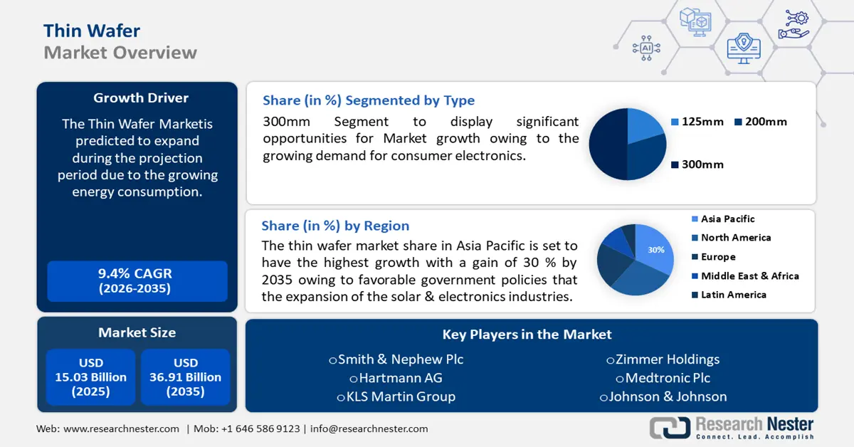
The growth of the market is propelled by the increasing generation of data. Every day, about 327 million terabytes of data are produced. To create microprocessors, memory chips, and other data processing and storing electrical devices, thin wafers are necessary. Thinner wafers allow manufacturers to create smaller, more energy-efficient devices that are better suited to handle enormous volumes of data.
The growing energy consumption also propels the demand for thin wafers. The total amount of US electricity used for end uses increased by 2.6% in 2022 compared to 2021. Retail power sales to the residential and commercial sectors increased by roughly 3.5% and 3.4%, respectively, in 2022 compared to 2021. Electronic devices made with thin wafers require less electricity to function than devices made with thicker wafers. This is for the reason that switching times may be sped up and power consumption may be reduced owing to the thinner dimensions of the transistors and other parts on the thin wafer.
Key Thin Wafer Market Insights Summary:
Regional Highlights:
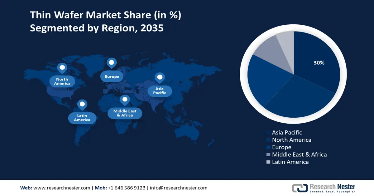
- Asia Pacific thin wafer market will hold over 30% share by 2035, driven by increasing adoption of smartphones, investment in R&D, expanding solar energy market, and favorable government policies for solar and electronics industries.
- North America market will achieve the highest CAGR during 2026-2035, driven by changes in automotive sector towards efficient and environmentally friendly vehicles, rising demand for cutting-edge automotive technology, and rapid expansion of medical equipment market.
Segment Insights:
- The 300mm wafers segment in the thin wafer market is expected to hold a 50% share by 2035, driven by growing consumer electronics demand and performance advantages of larger wafers.
- The leds segment in the thin wafer market is forecasted to hold the highest market share by 2035, fueled by the global phase-out of incandescent and fluorescent lighting in favor of LEDs.
Key Growth Trends:
- Growing Adoption of Smartphones
- Upsurge in Demand for Health Monitoring Devices
Major Challenges:
- Competition from Alternative Technologies
- Environmental Concerns
Key Players: Siltronic AG, SUMCO Corporation, My Chip Production GmbH, Global Wafers Co., Ltd., II-VI Incorporated, SunEdison Semiconductor Limited, 3M Company, Applied Material, Inc., Texas Instruments Incorporated.
Global Thin Wafer Market Forecast and Regional Outlook:
Market Size & Growth Projections:
- 2025 Market Size: USD 15.03 billion
- 2026 Market Size: USD 16.3 billion
- Projected Market Size: USD 36.91 billion by 2035
- Growth Forecasts: 9.4% CAGR (2026-2035)
Key Regional Dynamics:
- Largest Region: Asia Pacific (30% Share by 2035)
- Fastest Growing Region: Asia Pacific
- Dominating Countries: Taiwan, South Korea, China, United States, Japan
- Emerging Countries: China, India, South Korea, Thailand, Mexico
Last updated on : 10 September, 2025
Thin Wafer Market Growth Drivers and Challenges:
Growth Drivers
- Growing Adoption of Smartphones - About 85 percent of the world's population would own a smartphone by 2023 when there would be approximately 5 billion users worldwide. The microprocessors that make up the "brains" of cell phones are made on thin wafers. The thin wafer's reduced component sizes make it possible to create high-performance processors that could fit in the constrained space found in smartphones.
- Rise in Data Centers - In the entire world, there are about 7,999 data centers. Approximately 32% of the data centers among them are situated in the US. Hence, the demand for thin wafers is growing. Advanced cooling techniques for data centers, including the manufacture of heat sinks and thermal interface materials, are accomplished using thin wafers. The performance and dependability of the computer components in data centers must be maintained owing to the high heat generated by these facilities.
- Surge in Penetration of LEDs - Between 2012 and 2019, the pace of LED adoption in the global lighting industry increased, and in 2025, it is anticipated to reach a penetration of almost about 75 percent. Light-emitting diodes (LEDs), which are employed in a variety of lighting applications, are also produced on thin wafers.
- Rise in Demand for Renewable Sources of Energy - The percentage of renewable energy in the world's electrical generation increased from about 26% in 2019 to approximately 28% in 2020. Hence, the demand for solar chips is growing. When making solar cells, which turn sunlight into power, thin wafers are employed. The wafer's thinness enables more effective solar energy absorption and higher energy output.
- Upsurge in Demand for Health Monitoring Devices – Health monitoring gadgets, especially those that are wearable and implanted, are made from thin wafers. Hence, with the growing demand for health monitoring devices, the market is estimated to grow. Globally, the number of linked wearable devices has increased from 324 million in 2016 to approximately 721 million in 2019, more than doubling in only three years.
Challenges
- Competition from Alternative Technologies - Although thin wafers provide several advantages over thick wafers that have been used in the past, other technologies could also meet these demands. For instance, 3D packaging technology and cutting-edge materials could also make it possible to manufacture small, powerful gadgets. Hence, this factor is estimated to hinder the growth of the market.
- Environmental Concerns
- Lack of High Initial Investment
Thin Wafer Market Size and Forecast:
| Report Attribute | Details |
|---|---|
|
Base Year |
2025 |
|
Forecast Period |
2026-2035 |
|
CAGR |
9.4% |
|
Base Year Market Size (2025) |
USD 15.03 billion |
|
Forecast Year Market Size (2035) |
USD 36.91 billion |
|
Regional Scope |
|
Thin Wafer Market Segmentation:
Application Segment Analysis
The LEDs segment in the thin wafer market is anticipated to gamer the highest revenue by 2035. The growth of the segment is led by the growing production of LEDs. While many nations started phasing out incandescent bulbs more than 10 years ago, several are currently starting to do the same with fluorescent lighting so that LEDs eventually become the dominant lighting technology. The semiconductor layers in the LED are made from these wafers, which are subsequently cut into tiny chips. The performance of the LED could be influenced by the wafer's thickness. Employing thinner wafers, such as those constructed of GaN or SiC, may enhance the performance of the power components used in LEDs, including the switching speed, thermal conductivity, and breakdown strength.
Type Segment Analysis
The 300mm segment in the thin wafer market is expected to have significant growth with a share of 50 % during the forecast timeline. The segmental growth is credited to the growing demand for consumer electronics. The exponential use of 300 mm wafers in LED applications is fueling the growth of the market globally owing to the better performance offered by these wafers. A significant rise in demand for 300mm wafers is set to lead to an increase in the number of active 300mm wafer manufacturing facilities. Achieving economies of scale and raising the profitability of these wafers is becoming increasingly important for top LED makers. Additionally, the expansion of the 300mm wafer manufacturing sector is being aided by the increasing number of operational facilities.
Our in-depth analysis of the global thin wafer market includes the following segments:
|
Type |
|
|
Application |
|

Vishnu Nair
Head - Global Business DevelopmentCustomize this report to your requirements — connect with our consultant for personalized insights and options.
Thin Wafer Market Regional Analysis:
APAC Market Insights
The thin wafer market share in Asia Pacific is set to have the highest growth with a gain of 30 % by 2035. The adoption rate of smartphones reached about 73% in 2021 and is expected to increase to approximately 83 percent by 2025 in Asia Pacific. Increasing investment in R&D also propels regional market growth. With significant investments being made in solar energy infrastructure by nations including China, Japan, and India, the solar energy market is also expanding quickly in the Asia Pacific area. The manufacture of solar cells requires thin wafers, which are in high demand owing to the rising need for solar energy. Numerous nations in the Asia Pacific region, including China and India, have put favorable government policies into place to assist the expansion of the solar and electronics industries. The need for thin wafers is being fueled by these regulations, which offer incentives to firms to spend money on infrastructure and new technologies.
North American Market Insights
The North American thin wafer market is poised to have the highest growth during the forecast timeframe. With an emphasis on creating more effective and environmentally friendly automobiles such as electric vehicle, the North American automotive sector is going through considerable changes. The manufacturing of sensors and other parts for automobile systems including anti-lock brake systems (ABS), airbags, and engine control systems uses thin wafers. The rising demand for cutting-edge automotive technology also impels the market. A combination of an aging population and advancements in medical technology are fueling a rapid expansion of the North American market for medical equipment.
Thin Wafer Market Players:
- Siltronic AG
- Company Overview
- Business Strategy
- Key Product Offerings
- Financial Performance
- Key Performance Indicators
- Risk Analysis
- Recent Development
- Regional Presence
- SWOT Analysis
- SUMCO Corporation
- My Chip Production GmbH
- Global Wafers Co., Ltd.
- II-VI Incorporated
- SunEdison Semiconductor Limited
- 3M Company
- Applied Material, Inc.
- Texas Instruments Incorporated
Recent Developments
- A contract was inked by the Taiwanese company Global Wafers Co. Ltd. with the Munich-based Siltronic AG to establish a major wafer manufacturer. A “best-in-class” wafer producer was anticipated to be created by combining Siltronic, one of the technology leaders in the wafer industry, and GlobalWafers, with its excellent supply chain management and competitive cost structure, to compete successfully in the future global semiconductor market. It was anticipated that both firms’ product portfolios, which complement one another in several ways and serve as a solid foundation, would profit from the wafer industry's long-term growth drivers.
- A brand-new eBeam metrology system has been unveiled by Applied Materials, Inc., and it is especially made to measure exactly the crucial dimensions of semiconductor device features that have been patterned using EUV and the burgeoning High-NA EUV lithography.
- Report ID: 4882
- Published Date: Sep 10, 2025
- Report Format: PDF, PPT
- Explore a preview of key market trends and insights
- Review sample data tables and segment breakdowns
- Experience the quality of our visual data representations
- Evaluate our report structure and research methodology
- Get a glimpse of competitive landscape analysis
- Understand how regional forecasts are presented
- Assess the depth of company profiling and benchmarking
- Preview how actionable insights can support your strategy
Explore real data and analysis
Frequently Asked Questions (FAQ)
About this Report
Connect with our Expert

Report, 2026-2035


Copyright @ 2026 Research Nester. All Rights Reserved.
