Nano Metrology Market Outlook:
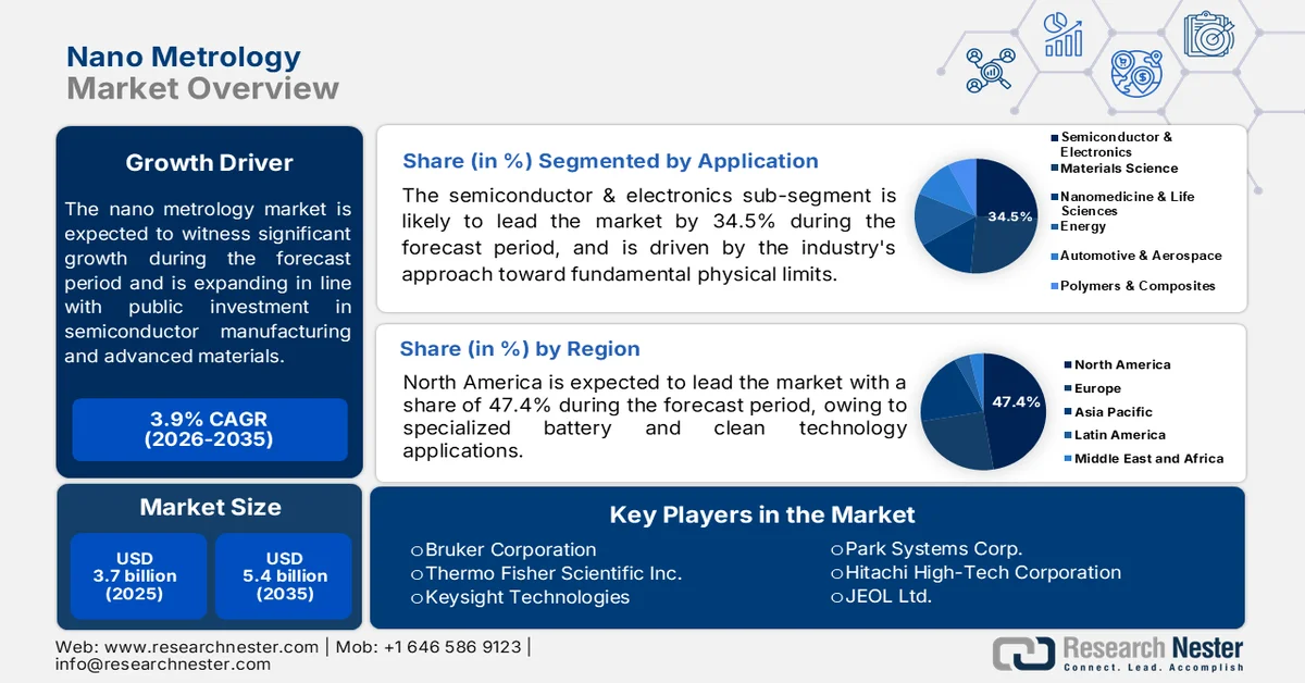
Nano Metrology Market size was valued at USD 3.7 billion in 2025 and is projected to reach USD 5.4 billion by 2035, rising at a CAGR of 3.9% during the forecast period, i.e., 2026-2035. In 2026, the industry size of nano metrology is assessed at USD 3.8 billion.
The nano metrology market demand is expanding in line with public investment in semiconductor manufacturing, advanced materials, quantum technologies, and precision healthcare manufacturing. According to the U.S. Department of Commerce, August 2024 data under the U.S. CHIPS and Science Act, the federal government authorized over USD 52 billion for semiconductor research, manufacturing, and workforce development, increasing the requirement for nanoscale inspection calibration and contamination analysis in the wafer fabrication facilities and packaging lines. The University of Calgary 2026 data shows that the European Commission’s Horizon Europe program allocated approximately USD 103.1 billion for research and innovation activities, with nanotechnology, advanced manufacturing, and industrial digitalization identified as priority areas. Growing adoption of high-precision metrology in medical device manufacturing, aerospace coatings, and battery materials is also strengthening long-term demand for traceable nanoscale measurement infrastructure and certified standards across regulated production environments.
Industrial scaling of advanced electronics and nanomaterials is further reinforcing the need for reliable nanoscale process validation and quality assurance. NIST and international standards organizations are also increasing activity around measurement interoperability, calibration, traceability, and nanomaterial characterization standards to support commercial deployment across cross-border supply chains. According to the NLM August 2022 study, both China and the U.S. have invested over USD 2 billion in nanotechnology worldwide. In healthcare and life sciences, nanoscale analytical systems are increasingly used in drug delivery research, biomaterials engineering, and molecular diagnostics manufacturing, particularly where regulatory compliance requires repeatable surface and structural analysis. These trends are positioning nano metrology as a critical enabling infrastructure layer for advanced manufacturing, precision engineering, and national technology development strategies.
Key Nano Metrology Market Insights Summary:
Regional Highlights:
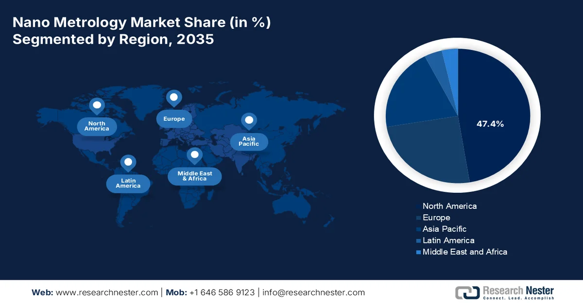
- North America nano metrology market is anticipated to account for 47.4% of the regional revenue share by 2035, attributed to rising deployment of atomic force microscopes and critical dimension scanning electron microscopes in semiconductor fabs for in-line process control
- Asia Pacific is forecast to witness a CAGR of 4.2% during 2026–2035 in the market, fueled by expanding semiconductor fabrication, display manufacturing, and battery production across Japan, South Korea, China, Taiwan, and Malaysia
Segment Insights:
- The semiconductor & electronics sub-segment is projected to capture 34.5% of the nano metrology market share by 2035, propelled by the increasing need for next-generation hybrid and non-destructive metrology solutions for sub-1nm semiconductor architectures
- The captive sub-segment is expected to dominate the market by 2035, impelled by semiconductor fabs deploying proprietary inline metrology systems for real-time quality control and advanced packaging defect detection
Key Growth Trends:
- National nanotechnology programs and public R&D investments
- Expansion of quantum technology research programs
Major Challenges:
- Extreme technological complexity
- Talent acquisition and language barriers
Key Players: Bruker Corporation (U.S.), Thermo Fisher Scientific Inc. (U.S.), Keysight Technologies (U.S.), Park Systems Corp. (South Korea), Hitachi High-Tech Corporation (Japan), JEOL Ltd. (Japan), Shimadzu Corporation (Japan), Oxford Instruments plc (UK), Nanosurf AG (Switzerland), Carl Zeiss AG (Germany), Attocube Systems AG (Germany), Nanonics Imaging Ltd. (Israel), Horiba, Ltd. (Japan), Semilab Semiconductor Physics Laboratory Co. Ltd. (Hungary), AIST-NT, Inc. (USA), Danish Micro Engineering A/S (Denmark), KLA Corporation (USA), SII NanoTechnology Inc. (Japan), • NanoMagnetics Instruments (Turkey), DeNovix (U.S.), Mitutoyo Corporation (Japan).
Global Nano Metrology Market Forecast and Regional Outlook:
Market Size & Growth Projections:
- 2025 Market Size: USD 3.7 billion
- 2026 Market Size: USD 3.8 billion
- Projected Market Size: USD 5.4 billion by 2035
- Growth Forecasts: 3.9% CAGR (2026-2035)
Key Regional Dynamics:
- Largest Region: North America (47.4% Share by 2035)
- Fastest Growing Region: Asia Pacific
- Dominating Countries: United States, China, Japan, South Korea, Taiwan
- Emerging Countries: India, Malaysia, Vietnam, Singapore, Thailand
Last updated on : 15 May, 2026
Nano Metrology Market - Growth Drivers and Challenges
Growth Drivers
- National nanotechnology programs and public R&D investments: Federal nanotechnology programs continue to drive the demand for advanced nanoscale measurement infrastructure across research institutions and industrial laboratories. As per the national nanotechnology initiative supplement to the president’s 2024 budget report, the national nanotechnology initiatives reported cumulative federal investment exceeding USD 43 billion since 2001, supporting nanoscale instrumentation, material characterization, and nanomanufacturing research. Agencies, including NIST, DOE, NIH, and NSF, fund projects requiring high-resolution imaging and dimensional analysis systems. Public laboratories increasingly require calibrated metrology systems capable of traceable and repeatable nanoscale measurements. These investments are encouraging partnerships between universities, government labs, and industrial manufacturers focused on nanoscale process validation.
- Expansion of quantum technology research programs: Quantum computing and quantum materials research programs are creating new demand for the ultra-high-resolution metrology tools capable of atomic-scale measurement and characterization. The U.S. National Quantum Initiative supports federal investments in quantum science research through agencies including NIST, DOE, and NSF. According to the CSIS June 2025 data, DOE has committed USD 575 million in quantum over 5 years. Quantum device fabrication requires nanoscale precision in material deposition, defect inspection, and thin-film measurement, driving demand for advanced microscopy and interferometric systems. The commercialization push for superconducting chips, quantum sensors, and photonic quantum devices is expected to increase procurement of nano metrology systems used for surface analysis and nanoscale dimensional verification in research and pilot manufacturing facilities.
- Growth in advanced battery and energy storage: The expansion of electric vehicle battery production and advanced energy storage systems is increasing reliance on nano metrology for electrode analysis, coating uniformity inspection, and nanomaterial characterization. The U.S. Department of Energy has committed billions of dollars toward domestic battery manufacturing and supply chain localization under clean energy programs. Battery materials such as lithium compounds, silicon anodes, and solid-state electrolytes require nanoscale structural validation to improve conductivity, thermal stability, and lifecycle performance. Nano metrology systems are increasingly used to evaluate particle morphology, nanoscale defects, and surface roughness in battery manufacturing environments.
Challenges
- Extreme technological complexity: Entering the nano metrology market requires mastery of multiple precision disciplines, optics, vibration control, piezo actuation, and sub-nanometer sensing. New players face a steep learning curve and must navigate dense patent landscapes dominated by the firms. Many Korean firms manufacture versions of equipment originally developed in the U.S. Japan or Europe, but struggle overseas where they lose cost advantage and run into intellectual property issues. High-tech companies often battle fiercely over patents, and many firms fear litigation.
- Talent acquisition and language barriers: For manufacturers in other nations, recruiting engineers with both deep technical expertise and fluency in language for global sales and support is extremely challenging in the nano metrology market. Large manufacturers can afford to hire persons speaking in their own regional language, but it's far more difficult for SMEs to hire engineers fluent in their regional language. This is a real obstacle that significantly hampers the engineering of global nano metrology market penetration for otherwise technologically capable firms.
Nano Metrology Market Size and Forecast:
| Report Attribute | Details |
|---|---|
|
Base Year |
2025 |
|
Forecast Year |
2026-2035 |
|
CAGR |
3.9% |
|
Base Year Market Size (2025) |
USD 3.7 billion |
|
Forecast Year Market Size (2035) |
USD 5.4 billion |
|
Regional Scope |
|
Nano Metrology Market Segmentation:
Application Segment Analysis
The semiconductor & electronics sub-segment dominates the nano metrology market and is expected to capture the share value of 34.5% by the end of 2035. The segment is driven by the industry's approach toward fundamental physical limits. According to the NLM July 2025 data, the integrated circuits transition from planar to 3D stacked architectures with sub-1nm features and layer counts exceeding 200. Conventional techniques, such as Atomic Force Microscopy (AFM) and Critical Dimension Scanning Electron Microscopy (CD-SEM), face an inherent conflict between accuracy, speed, and non-destructiveness. This metrology bottleneck directly determines chip performance yield and manufacturability for Angstrom-scale nodes. Moreover, the semiconductor fabs reported an increase in metrology-related rework due to inadequate resolution for buried 3D structures, accelerating demand for next-generation hybrid and non-destructive nano-metrology solutions capable of probing high-aspect-ratio features without damaging delicate heterogeneous materials.
Trade Segment Analysis
Under the trade segment, the captive sub-segment is leading and is poised to hold the largest share value by the end of 2035 in the nano metrology market. Captive holds the largest share because semiconductor fabs require real‑time, proprietary quality control. According to the NIST January 2025 data, the CHIPS NAPMP’s USD 300 million award to Absolics Applied Materials and Arizona State University for advanced substrates and packaging, aiming to establish high‑volume domestic packaging where chips are both manufactured and packaged in the U.S. These new fabs will deploy inline captive metrology (AFM, CD‑SEM) for glass core flatness and bridge defect detection, avoiding merchant lab delays. NIST reported that captive nano‑metrology installations in U.S. advanced packaging fabs have further increased the government‑backed scale‑up.
End user Segment Analysis
Within the nano metrology market, semiconductor fabs represent the largest end‑user segment. These facilities operate 24/7 production lines where inline nano‑metrology directly controls yield and process stability. Fabs deploy atomic force microscopes, critical dimension scanning electron microscopes, and optical scatterometers to measure gate height, spacer thickness, contact hole circularity, and edge placement error at multiple process steps, including lithography, etching, and chemical mechanical planarization. The transition to gate‑all‑around transistors, backside power delivery, and advanced packaging has increased the number of metrology steps per wafer. Semiconductor fabs prioritize high‑speed non‑destructive and automated nano‑metrology tools that integrate seamlessly with fab execution systems, enabling real‑time process adjustments and defect review without slowing production throughput.
Our in-depth analysis of the nano metrology market includes the following segments:
|
Segment |
Subsegments |
|
Product Type |
|
|
Technology |
|
|
Application |
|
|
End user |
|
|
Component |
|
|
Trade |
|

Vishnu Nair
Head - Global Business DevelopmentCustomize this report to your requirements — connect with our consultant for personalized insights and options.
Nano Metrology Market - Regional Analysis
North America Market Insights
The North America nano metrology market is the largest and is poised to hold the regional revenue share of 47.4% by 2035. The region is driven by the U.S., with Canada contributing via specialized battery and clean technology applications. Semiconductor fabs represent the largest end-user segment requiring atomic force microscopes and critical dimension scanning electron microscopes for in-line process control. Government initiatives focused on domestic microscopes for in-line process control. Government initiatives focused on domestic advanced packaging and substrate research have stimulated captive metrology adoption, where fabs perform measurements internally rather than outsourcing. The nano metrology market continues transitioning from research-oriented instruments to high-throughput production tools designed for 24/7 manufacturing environments, with end users prioritizing measurement speed and repeatability over ultimate resolution.
The increasing investments in AI-focused semiconductor manufacturing, advanced packaging, and precision optical measurement technologies are shaping the nano metrology market in the U.S. In September 2025, Onto Innovation introduced the Atlas® G6 optical critical dimension metrology system to support next-generation gate-all-around (GAA) logic and high bandwidth memory (HBM) production, where structural dimensions are shrinking by nearly 30% per generation. Applied Materials in October 2025 also launched new semiconductor manufacturing platforms targeting advanced logic, DRAM, and packaging technologies required for AI computing, increasing demand for nanoscale process control and inspection systems across U.S. fabs. These developments reflect expanding domestic demand for the high-precision nanoscale measurement infrastructure tied to the semiconductor localization and AI hardware production.
The expanding investments in quantum technologies, precision manufacturing, and advanced analytical instrumentation are shaping the nano metrology market in Canada. According to the Government of Canada, April 2026 data, the country’s quantum sector could reach USD 139 billion and generate more than 200,000 jobs by 2045, increasing the demand for the nanoscale characterization and measurement systems used in the quantum device fabrication and materials research. Canada also invested more than USD 1 billion in quantum science initiatives, and provincial governments and private investors committed an additional USD 1 billion toward quantum innovation and commercialization. On the other hand, in January 2026, Hitachi High Tech is expanding advanced analytical instrumentation offerings, strengthening demand for precision metrology and quality-control technologies across semiconductor, photonics, and industrial manufacturing applications in Canada.
APAC Market Insights
The Asia Pacific is projected to emerge as the fastest-growing region in the nano metrology market and is poised to grow at a CAGR of 4.2% during the assessed period, 2026 to 2035. The region is driven by concentrated semiconductor fabrication, display manufacturing, and battery production across Japan, South Korea, China, Taiwan, and Malaysia. Japan and South Korea lead in high-resolution atomic force microscopy and critical dimension scanning electron microscopes, and China emphasizes the localization of metrology tools for domestic fabs. Emerging Southeast Asian hubs, mainly Malaysia and Vietnam, are adopting cost-optimized optical profilometers for outsourced assembly and test operations. India contributes via merchant metrology services for its growing electronics manufacturing ecosystem. Hybrid metrology combining multiple techniques on a single platform is gaining traction for advanced packaging inspection.
Expanding large-scale government investments in quantum technologies, semiconductor research, and advanced manufacturing infrastructure is fueling the nano metrology market in India. According to the PIB December 2025 data, the National Quantum Mission, approved with an outlay of USD 720 million, is supporting quantum sensing fabrication facilities and indigenous quantum device development across premier institutions, including IISc Bengaluru and IITs. In addition, the Government of India approved the USD 12 billion Research, Development, and Innovation Scheme in 2025 to accelerate private-sector R&D in semiconductors, AI, biotechnology, robotics, and deep-tech industries that require nanoscale characterization and process-control systems. Research institutions such as the Institute of Nano Science and Technology (INST) and CeNS are also advancing nanomedicine, nano-catalysts, smart materials, and energy-storage technologies, increasing demand for high-resolution nano metrology and precision analytical instruments across India’s research and industrial sectors.
India Nano Metrology Market Growth
|
Growth Indicator |
Statistics / Development |
|
National Quantum Mission (NQM) |
₹6,003.65 crore government allocation for 8 years |
|
Research, Development & Innovation (RDI) Scheme |
₹1 lakh crore approved in 2025 |
|
Central Fabrication Facilities |
₹720 crore investment across IIT Delhi, IISc Bengaluru, IIT Bombay, and IIT Kanpur |
|
Global Innovation Ranking |
India ranked 38th in Global Innovation Index 2025 |
|
Quantum Technology Startups |
8 startups supported under NQM |
|
Research Infrastructure Expansion |
₹273.89 crore approved under FIST 2024 for 115 departments and 22 PG colleges |
|
Supercomputing Infrastructure |
39 petaflop supercomputers installed across 37 locations |
|
Precision Manufacturing Support |
11 projects funded under Advanced Manufacturing Technologies program |
Source: PIB December 2025
The Japan nanometrology market is expanding rapidly and reached USD 970 million in 2025 and is estimated to reach USD 1,760 million by the end of 2035 during the forecast period of 2026–2035. In 2026, the market is projected to reach USD 1,060 million. The nation is driven by the strong investments in semiconductor manufacturing, quantum technologies, and advanced material research. According to the SEMI August 2025 data, nearly USD 26 billion is needed to strengthen domestic semiconductor and AI infrastructure development. The Japan Times November 2024 data indicated that the government also committed approximately USD 7 billion for Rapidus and next-generation chip production initiatives requiring nanoscale process-control systems. In addition, these data support the demand for high-resolution nanoscale characterization and metrology tools across semiconductor, photonics, and precision manufacturing sectors.
Europe Market Insights
The nano metrology market in Europe is defined by a strong presence of research institutes, precision optics manufacturers, and specialized instrument developers. Germany, Switzerland, and the UK host leading companies focusing on optical profilers, interferometers, and hybrid metrology systems. Academic and government research centers serve as early adopters, often collaborating with instrument manufacturers through public-private partnerships. Emerging trends include portable nano-profilometers for on-site quality control, harmonized calibration standards across EU member states, and metrology for silicon photonics and MEMS devices. The market favors the modular application-specific configurations over high-throughput production tools, reflecting Europe's diverse industrial base and emphasis on precision engineering excellence.
The growing investments in nanofabrication, quantum technologies, and advanced materials research are shaping the nano metrology market in Germany. In October 2024, Heidelberg Instruments recently introduced its NanoFrazor nanolithography platform in Heidelberg, designed for quantum devices, nanoscale electronics, nanophotonics, and 2D material applications requiring high-resolution nanoscale patterning and characterization. The system’s ability to integrate multiple parallel cantilevers reflects rising industrial demand for higher-throughput precision nanomanufacturing tools. Germany is also strengthening the commercialization of nanotechnology-enabled clean energy solutions through initiatives such as Project NanoPEC, in June 2023, a three-year collaboration involving SunHydrogen and six German industry and research partners focused on renewable hydrogen technologies. These developments are increasing demand for nanoscale inspection, thin-film analysis, and process-control systems across Germany’s semiconductor, energy photonics, and industrial research sectors, supporting continued market growth through advanced manufacturing investments.
The increasing commercialization of nanomaterials and nanotechnology-enabled products across various sectors is driving the nano metrology market in the UK. Rising adoption of nanomaterials with enhanced electrical, optical, and surface properties is increasing the demand for nanoscale characterization, dimensional analysis, and quality control systems in the research and production environments. Global growth in the nanotechnology-enabled consumer products further supports this trend, with the Nanotechnology Consumer Products Index expanding from 54 products in to 1,814 products, while the Danish Nanodatabase increased from 1,206 products in 2012 to 5,224 products in 2021, as per the UK Government’s November 2024 data. These developments are strengthening demand in the UK for advanced nano metrology tools used in semiconductor materials, nanophotonics, biomaterials, and precision manufacturing applications requiring high-resolution measurement and process validation capabilities.
Number of Products Containing Nanomaterials, 2012-2022
|
Year |
Number of Products |
|
2012 |
1208 |
|
2013 |
1213 |
|
2014 |
1421 |
|
2015 |
2281 |
|
2016 |
2445 |
|
2017 |
3423 |
|
2018 |
3558 |
|
2019 |
4146 |
|
2020 |
5000 |
|
2021 |
5286 |
|
2022 |
5286 |
Source: UK Government November 2024
Key Nano Metrology Market Players:
- Bruker Corporation (U.S.)
- Thermo Fisher Scientific Inc. (U.S.)
- Keysight Technologies (U.S.)
- Park Systems Corp. (South Korea)
- Hitachi High-Tech Corporation (Japan)
- JEOL Ltd. (Japan)
- Shimadzu Corporation (Japan)
- Oxford Instruments plc (UK)
- Nanosurf AG (Switzerland)
- Carl Zeiss AG (Germany)
- Attocube Systems AG (Germany)
- Nanonics Imaging Ltd. (Israel)
- Horiba, Ltd. (Japan)
- Semilab Semiconductor Physics Laboratory Co. Ltd. (Hungary)
- AIST-NT, Inc. (USA)
- Danish Micro Engineering A/S (Denmark)
- KLA Corporation (USA)
- SII NanoTechnology Inc. (Japan)
- NanoMagnetics Instruments (Turkey)
- DeNovix (U.S.)
- Mitutoyo Corporation (Japan)
- Company Overview
- Business Strategy
- Key Product Offerings
- Financial Performance
- Key Performance Indicators
- Risk Analysis
- Recent Development
- Regional Presence
- SWOT Analysis
- Bruker Corporation is a dominant player in the nano metrology market, offering advanced atomic force microscopy and nanoindentation systems that enable high-resolution surface characterization at the sub-nanometer scale. The company has significantly advanced the market by integrating high-speed scanning and automated analytics into its Dimension and Innova series. According to the 2024 annual report, the company has made revenue of USD 979.6 million in Q4 2024.
- Thermo Fisher Scientific Inc. has cemented its leadership in the nano metrology market via its suite of scanning electron microscopes and dual beam focused ion beam systems with nanoprobing capabilities. The company has advanced the market by embedding real-time nano geometrical metrology into its Verios and HeliScan platforms, enabling correlative imaging and elemental analysis. In 2025, the company made a revenue of USD 44.56 billion.
- Keysight Technologies is a key innovator in the nano metrology market, primarily via its high-precision atomic force microscopy and scanning probe microscopy solutions for electrical characterization at the nanoscale. The company has advanced the market by embedding nano-electrical metrology into compact, user-friendly devices that enable real-time current mapping and capacitance profiling.
- Park Systems Corp., headquartered in South Korea, has emerged as the leading specialist in the nano metrology market, renowned for its true non-contact atomic force microscopy technology that preserves tip and sample integrity. The company has advanced the market by embedding cross-platform automation and real-time vibration cancellation into its NX series systems, enabling high-speed scanning for semiconductor pattern analysis and precision.
- Hitachi High Tech Corporation is a stalwart player in the nano metrology market, offering versatile scanning electron microscopes and atomic force microscopes customized for industrial quality assurance and life sciences. The company has advanced the nano metrology market by integrating low-voltage, high-resolution imaging and automated features, enabling observation of fine nanostructures without damaging electron-sensitive specimens.
Here is a list of key players operating in the global nano metrology market:
The nano metrology market is highly consolidated and is driven by the demand from the semiconductor, materials science, and biomedical sectors. The key players focus on strategic initiatives such as launching hybrid systems, forming R&D collaborations with academic institutions, and expanding the aftermarket services. Moreover, companies are entering into a strategic partnership to expand their geographical reach. For example, in August 2025, Park Systems Corp. announced the acquisition of Swiss-based Lyncée Tec SA. Companies from the U.S. and Japan lead in the ultra-high-resolution systems, and Europe firm specialize in optical and interferometric solutions. To gain a share, the emerging players from South Korea and Malaysia highlight the cost-effective modules and regional service hubs. IP litigation and patent cross licensing remain common competitive tactics to protect core sensing technologies.
Corporate Landscape of the Nano Metrology Market:
Recent Developments
- In June 2025, Bruker Corporation announced the shipment and installation of the 15th InSight WLI 3D optical metrology system to a leading semiconductor manufacturer. The installation is part of a larger order from this semiconductor manufacturer for 27 Bruker optical metrology systems in 2025. This reflects the growing demand for high-performance metrology that can support advanced packaging requirements in the latest generation AI high-performance chip manufacturing processes.
- In March 2025, DeNovix introduced the Helium 1 µL Spectrophotometer, a new nanovolume spectrophotometer in the DS-Series Quantification Range. At a price accessible to all labs, the Helium 1 µL Spectrophotometer delivers quality performance and reliable quantification of 1 µL nucleic acids and protein samples. This stand-alone device includes a 7” HD touchscreen with simple, easy-to-use software.
- In December 2024, Park Systems, a leading manufacturer of nano-metrology systems, announced the release of its latest atomic force microscopy (AFM) innovation, Park FX200, designed for 200 mm samples. The FX200 is developed to meet the needs of both research and industrial applications, offering significant advancements in large-sample AFM technology.
- Report ID: 7469
- Published Date: May 15, 2026
- Report Format: PDF, PPT
- Explore a preview of key market trends and insights
- Review sample data tables and segment breakdowns
- Experience the quality of our visual data representations
- Evaluate our report structure and research methodology
- Get a glimpse of competitive landscape analysis
- Understand how regional forecasts are presented
- Assess the depth of company profiling and benchmarking
- Preview how actionable insights can support your strategy
Explore real data and analysis
Frequently Asked Questions (FAQ)
Nano Metrology Market Report Scope
Free Sample includes current and historical market size, growth trends, regional charts & tables, company profiles, segment-wise forecasts, and more.
Connect with our Expert


Copyright @ 2026 Research Nester. All Rights Reserved.
