Atomic Force Microscopy Market Outlook:
Atomic Force Microscopy Market size was estimated at USD 586.3 million in 2025 and is expected to surpass USD 973.3 million by the end of 2035, rising at a CAGR of 5.2% during the forecast period, i.e., 2026-2035. In 2026, the industry size of atomic force microscopy is evaluated at USD 616.7 million.
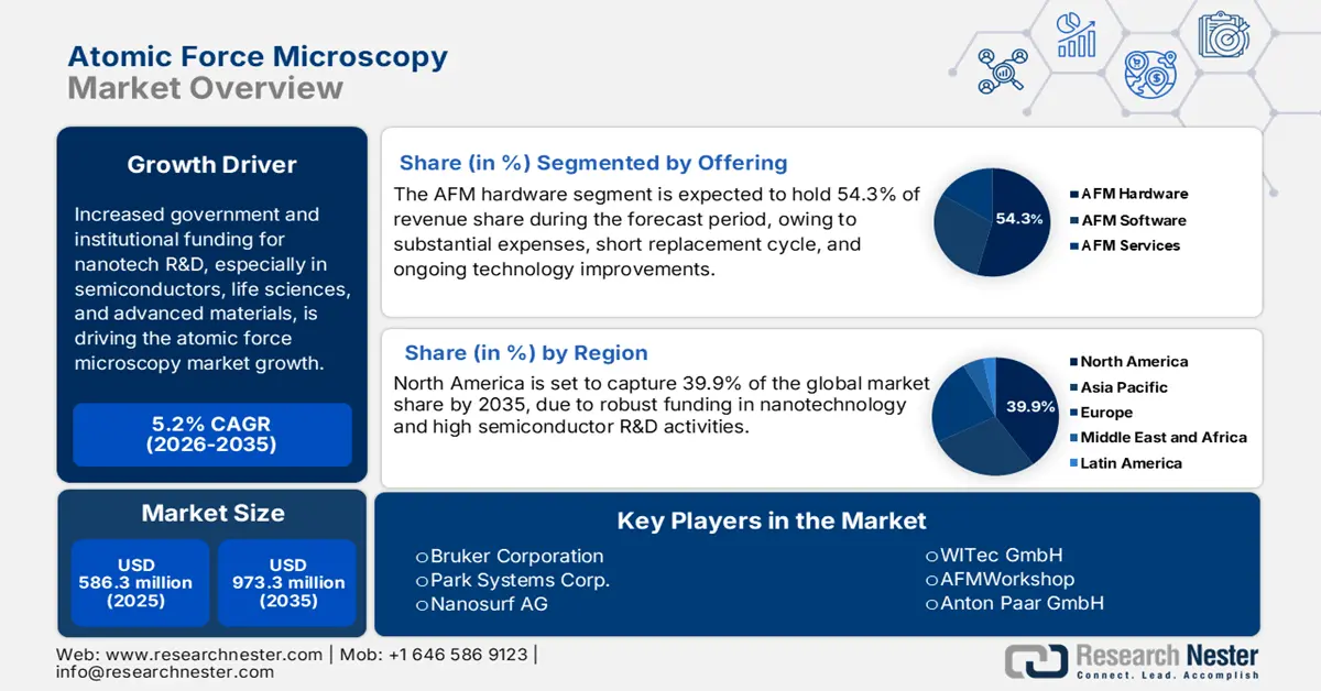
The increasing government and institutional funding for nanotech R&D, especially in semiconductors, life sciences, and advanced materials, is driving the atomic force microscopy (AFM) market. For example, the U.S. government spent more than USD 1.9 billion on nanotechnology-related R&D in 2023, while the European Commission's Horizon Europe program is spending approximately €7.3 billion, academically and industrially, on cutting-edge science, green and digital science. Such investment moves are resulting in the commercialization of AFM in academic, industrial, and government labs, including both domestic and export-oriented, particularly for semiconductor metrology, and for biomedical uses that require nanoscale precision.
|
Organization/Program/Initiative |
What it is |
How It Works (Mechanism) |
Nanotech Commercialization Role |
|
Federal Laboratory Consortium (FLC) |
Nationwide network of 300+ federal labs, agencies, and research centers |
Tech transfer network; one-stop shop for labs, available technologies, funding, programs, facilities |
Accelerates moving federally developed nanotechnologies from labs to market |
|
IN-Q-TEL |
Non-profit strategic investor supporting U.S. Government agencies |
Strategic investment and transition of startup technologies to national security users |
Funds/accelerates nano-enabled solutions with defense/security applications |
|
Manufacturing USA |
Public-private network of advanced manufacturing institutes |
Collaborative R&D, technology transition, workforce training, supply-chain development |
Scales nano-enabled products/processes in the U.S.; builds domestic manufacturing capacity |
|
SBA FAST Partnership Program |
Governed by the U.S. Small Business Administration (SBA) |
Competitive grants to strengthen small tech firms’ commercialization capabilities |
Increases small-business participation in nanotech innovation and market entry |
Source: National Nanotechnology Institute
Key Atomic Force Microscopy Market Insights Summary:
Regional Highlights:
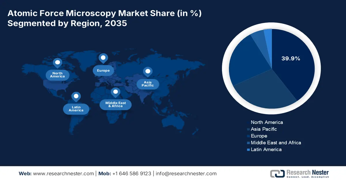
- North America is expected to hold 39.9% share through 2035, driven by increased nanotechnology funding, semiconductor R&D, and academic collaborations.
- Asia Pacific is projected to hold 28.1% share during the study period, owing to booming investments in semiconductor and material research.
Segment Insights:
- AFM hardware segment is estimated to garner 54.3% share during the projected period, driven by ongoing technology improvements, high costs, and increasing investment in nanomechanical research.
- Semiconductors segment is anticipated to capture 41.8% share, propelled by rising R&D spending and the demand for precise 3D nanostructure characterization in advanced chip fabrication.
Key Growth Trends:
- Growth in life sciences applications
- Industry 4.0 and smart manufacturing trends
Major Challenges:
- High production & operational costs due to safety regulations
- Market access barriers and export restrictions
Key Players: Bruker Corporation, Park Systems Corp., Oxford Instruments Asylum Research, Hitachi High-Tech Corporation, Nanosurf AG, NT-MDT Spectrum Instruments, JPK Instruments AG (a Bruker Company), WITec GmbH, AFMWorkshop, Anton Paar GmbH, Advanced Surface Microscopy, Inc., A.P.E. Research srl, Nanonics Imaging Ltd., Pacific Nanotechnology, Inc., Quantum Design Japan, Inc.
Global Atomic Force Microscopy Market Forecast and Regional Outlook:
Market Size & Growth Projections:
- 2025 Market Size: USD 586.3 million
- 2026 Market Size: USD 616.7 million
- Projected Market Size: USD 973.3 million by 2035
- Growth Forecasts: 5.2% CAGR (2026-2035)
Key Regional Dynamics:
- Largest Region: North America (39.9% Share)
- Fastest Growing Region: Europe
- Dominating Countries: United States, Germany, Japan, South Korea, France
- Emerging Countries: China, India, Taiwan, Singapore, Australia
Last updated on : 2 September, 2025
Atomic Force Microscopy Market - Growth Drivers and Challenges
Growth Drivers
- Growth in life sciences applications: The atomic force microscopy is gaining traction in life sciences, in biophysics, molecular diagnostics, and cellular mechanics. Many researchers prefer atomic force microscopy technologies owing to their advanced nanoscale resolution. Moreover, the vital role of AFM in drug development, disease diagnostics, and personalized medicine is projected to fuel its sales growth and job opportunities in the years ahead. The U.S. Bureau of Labor Statistics states that jobs in life, physical, and social sciences are expected to increase at a higher rate than most other jobs from 2023 to 2033. On average, about 148,400 job openings are estimated each year.
- Industry 4.0 and smart manufacturing trends: The Industry 4.0 trend is expected to positively influence the sales of atomic force microscopy technologies. In semiconductor and nanomanufacturing environments, atomic force microscopy solutions are widely used for inline, high-resolution surface characterization needs. In August 2025, Appl, Inc. revealed a new USD 100 billion investment in U.S. manufacturing, adding to its existing plans, bringing the total to USD 600 billion over the next four years. Such moves in the manufacturing sector are opening lucrative earning opportunities for AFM manufacturers. Furthermore, the continuous technological advancements coupled with the integration of automation, IoT, and predictive analytics are expected to accelerate the production and commercialization of smart atomic force microscopy technologies.
- Increasing adoption in diagnostics: The healthcare sector is emerging as one of the most promising end users for atomic force microscopy technologies. The diagnostics sector is particularly pushing the sales of atomic force microscopy solutions, owing to their ability to capture high-resolution, three-dimensional images of biomolecules, cells, and tissues. Additionally, the rising prevalence of chronic disorders and innovations in diagnostic technologies are further fueling the trade of AFMs. This statement is supported by the World Health Organization’s (WHO) 2024 report on Noncommunicable Diseases. The source states that around 82% of the individuals in the low- and middle-income countries are more susceptible to noncommunicable diseases, also known as chronic disorders. Further, the Centers for Disease Control and Prevention (CDC) in its October 2024 report states that in the U.S., chronic diseases are the leading cause of illness and disability. Thus, for diagnostics and treatment needs, atomic force microscopy technologies are projected to exhibit high application.
Challenges
- High production & operational costs due to safety regulations: The strict safety regulations, such as the Environmental Protection Agency’s (EPA) Toxic Substances Control Act (TSCA), increase the operational costs and make it more challenging for small companies and start-ups. Also, lower budgets limit the expansion of domestic manufacturing units in the developing regions. Some manufacturers miss commercial launch deadlines due to the additional costs of compliance.
- Market access barriers and export restrictions: Barriers to adherence and compliance in the form of non-tariff barriers (NTBs), such as local testing and approval requirements, are keeping AFM exports down, especially to developing countries such as India, Brazil, and China. Many companies faced months of delay due to being governed by the new safety standards for all imported nanotechnology-based instruments. Thus, tariff barriers are expected to hinder the sales of atomic force microscopy solutions to some extent.
Atomic Force Microscopy Market Size and Forecast:
| Report Attribute | Details |
|---|---|
|
Base Year |
2025 |
|
Forecast Year |
2026-2035 |
|
CAGR |
5.2% |
|
Base Year Market Size (2025) |
USD 586.3 million |
|
Forecast Year Market Size (2035) |
USD 973.3 million |
|
Regional Scope |
|
Atomic Force Microscopy Market Segmentation:
Offering Segment Analysis
The AFM hardware segment is estimated to garner the largest atomic force microscopy market share of 54.3% during the projected period, due to its substantial expense, short replacement cycle, and ongoing technology improvements. ABM hardware consists of cantilevers, scanners, and high-resolution probes. Increased investment in nanomechanical science, especially in semiconductors and materials, is creating demand for new AFM instrumentation. In September 2023, the National Institutes of Health (NIH) revealed the launch of a USD 2 million competition to boost research and development in fetal diagnostic and monitoring technologies. Such funding initiatives are expected to boost the production of advanced hardware components in the diagnostic solutions, including atomic force microscopes.
Application Segment Analysis
The semiconductors segment is anticipated to capture 41.8% of the global atomic force microscopy market share, mainly due to the process nodes for chips being <5nm. AFM provides an important measurement capability to analyze the 3D nanostructure under development and to inspect line-edge roughness. The R&D spending is growing globally as the demand for new, improved AFM characterization tools used for semiconductor fabrication is increasing. The non-destructive imaging provided by AFM is extremely valuable when there are overlays of sensitive thin films and dopants in next-generation transistors and sensors.
Grade Segment Analysis
The industrial-grade segment is foreseen to hold a dominant share of the atomic force microscopy market, due to its widespread use in high-value sectors such as semiconductors, materials science, and nanomanufacturing. Precision, speed, and reliability in production environments are also making industrial-grade AFM more demanding. The semiconductor, nanotechnology, and renewable energy sectors are mainly driving the sales of industry-grade AFMs. The robust automation and IoT integration are likely to accelerate the trade of industrial-grade atomic force microscopies in the years ahead.
Our in-depth analysis of the atomic force microscopy market includes the following segments:
|
Segments |
Subsegments |
|
Offering |
|
|
Application |
|
|
Type |
|
|
Grade |
|

Vishnu Nair
Head - Global Business DevelopmentCustomize this report to your requirements — connect with our consultant for personalized insights and options.
Atomic Force Microscopy Market - Regional Analysis
North America Market Insights
The North America atomic force microscopy market is expected to hold 39.9% of the global revenue share through 2035, due to an increase in nanotechnology funding and semiconductor R&D, as well as collaborations with leading academic institutions. The U.S. National Nanotechnology Initiative's funding of over USD 45 billion is expected to drive the sales of atomic force microscopy solutions. The growing demand in aerospace, pharma, and electronics, in conjunction with emerging trends, such as 2D materials and high-speed imaging, is also set to boost the adoption of AFMs.
The U.S. leads the sales of atomic force microscopes owing to the fabs, defense-linked materials programs, and deep life sciences funding. High semiconductor production and innovation in diagnostics & nanotechnology are poised to propel the sales of atomic force microscopy technologies. The Federal Reserve Bank of St. Louis states that the producer price index for semiconductor and other electronic component manufacturing stood at 57.467 in July 2025. The pricing changes and continuous innovations are driving the sales of atomic force microscopes.
Asia Pacific Market Insights
The Asia Pacific atomic force microscopy market is expected to hold 28.1% of the global revenue share throughout the study period, owing to the booming investments in semiconductor and material research. China is a leading marketplace due to the massive government investments in nanotechnology and chip fabrication. Japan and South Korea are also driving the regional demand, with AFM adoption in 2D materials research. Further, Taiwan's semiconductor industry leads premium AFM sales for sub-3nm node development (TSIA).
The China atomic force microscopy market is projected to be driven by semiconductor and advanced materials research. The government-backed investments in semiconductors, nanotechnology, and life sciences are set to boost the sales of atomic force microscopy solutions. The country’s Made in China 2025 strategy and subsequent policies supporting self-reliance in high-tech manufacturing are attracting international atomic force microscopy investors. Industrial automation is another factor poised to double the revenues of key players in the years ahead.
Europe Market Insights
The Europe atomic force microscopy market is set to increase at the fastest CAGR from 2026 to 2035, owing to its strong academic research ecosystem and advanced materials science capabilities. The steady semiconductor supply chain and continuous investments in technological advancements are also contributing to the increasing sales of atomic force microscopy solutions. Furthermore, Europe’s emphasis on sustainability and clean energy fuels is likely to accelerate the production and commercialization of smart atomic force microscopy technologies.
Germany holds a leading share in Europe’s atomic force microscopy market, due to the strong concentration of semiconductor players and research universities. The expanding materials science industry is also propelling the trade of atomic force microscopy solutions. The government R&D programs under the High-Tech Strategy 2025, which prioritize nanotechnology and digitalization, are further expected to promote the expansion of AFM manufacturing units of both domestic and international players.
Key Atomic Force Microscopy Market Players:
- Bruker Corporation
- Company Overview
- Business Strategy
- Key Product Offerings
- Financial Performance
- Key Performance Indicators
- Risk Analysis
- Recent Development
- Regional Presence
- SWOT Analysis
- Park Systems Corp.
- Oxford Instruments Asylum Research
- Hitachi High-Tech Corporation
- Nanosurf AG
- NT-MDT Spectrum Instruments
- JPK Instruments AG (a Bruker Company)
- WITec GmbH
- AFMWorkshop
- Anton Paar GmbH
- Advanced Surface Microscopy, Inc.
- A.P.E. Research srl
- Nanonics Imaging Ltd.
- Pacific Nanotechnology, Inc.
- Quantum Design Japan, Inc.
The leading companies in the market are employing both organic and inorganic strategies to earn lucrative gains. Key players are focused on the production of innovative atomic force microscopy solutions to attract a wider consumer base. The industry giants are also engaging in mergers, acquisitions, collaborations, and partnerships to increase their market reach and product line. Further, some big players are expanding their operations in the developing markets to earn high profits from untapped opportunities.
Some of the key players operating in the atomic force microscopy market are listed below:
Recent Developments
- In June 2025, Park Systems hosted a global interactive online showcase for the Park FX Large Sample AFM Series. In this event, the company introduced its product line, including the Park FX200, FX300, FX200 IR, and FX300 IR.
- In January 2025, Iowa State University announced that Juan Ren, Adarsh Krishnamurthy, Anwesha Sarkar, and Aditya Balu received a USD 1 million grant from the National Science Foundation. They are set to use it to develop a new system that combines artificial intelligence and machine learning to improve atomic force microscopy capabilities.
- In December 2024, Bruker Corporation announced the launch of its Dimension Nexus atomic force microscope system. This solution offers an optimal intersection of performance and value for the evolving needs of both growing labs and multi-user facilities.
- Report ID: 5250
- Published Date: Sep 02, 2025
- Report Format: PDF, PPT
- Explore a preview of key market trends and insights
- Review sample data tables and segment breakdowns
- Experience the quality of our visual data representations
- Evaluate our report structure and research methodology
- Get a glimpse of competitive landscape analysis
- Understand how regional forecasts are presented
- Assess the depth of company profiling and benchmarking
- Preview how actionable insights can support your strategy
Explore real data and analysis
Frequently Asked Questions (FAQ)
Atomic Force Microscopy Market Report Scope
Free Sample includes current and historical market size, growth trends, regional charts & tables, company profiles, segment-wise forecasts, and more.
Connect with our Expert


Copyright @ 2026 Research Nester. All Rights Reserved.
